
Cerebras: The $56.4 Billion IPO Challenging NVIDIA’s Memory Wall
The physics behind wafer-scale AI chips, why they make LLM decode faster, and why capacity, software, and unit economics may still decide the company’s fate.

It takes time to create work that’s clear, independent, and genuinely useful. If you’ve found value in this newsletter, consider becoming a paid subscriber. It helps me dive deeper into research, reach more people, stay free from ads/hidden agendas, and supports my crippling chocolate milk addiction. We run on a “pay what you can” model—so if you believe in the mission, there’s likely a plan that fits (over here).
Every subscription helps me stay independent, avoid clickbait, and focus on depth over noise, and I deeply appreciate everyone who chooses to support our cult.
PS – Supporting this work doesn’t have to come out of your pocket. If you read this as part of your professional development, you can use this email template to request reimbursement for your subscription.
Every month, the Chocolate Milk Cult reaches over a million Builders, Investors, Policy Makers, Leaders, and more. If you’d like to meet other members of our community, please fill out this contact form here (I will never sell your data nor will I make intros w/o your explicit permission)- https://forms.gle/Pi1pGLuS1FmzXoLr6
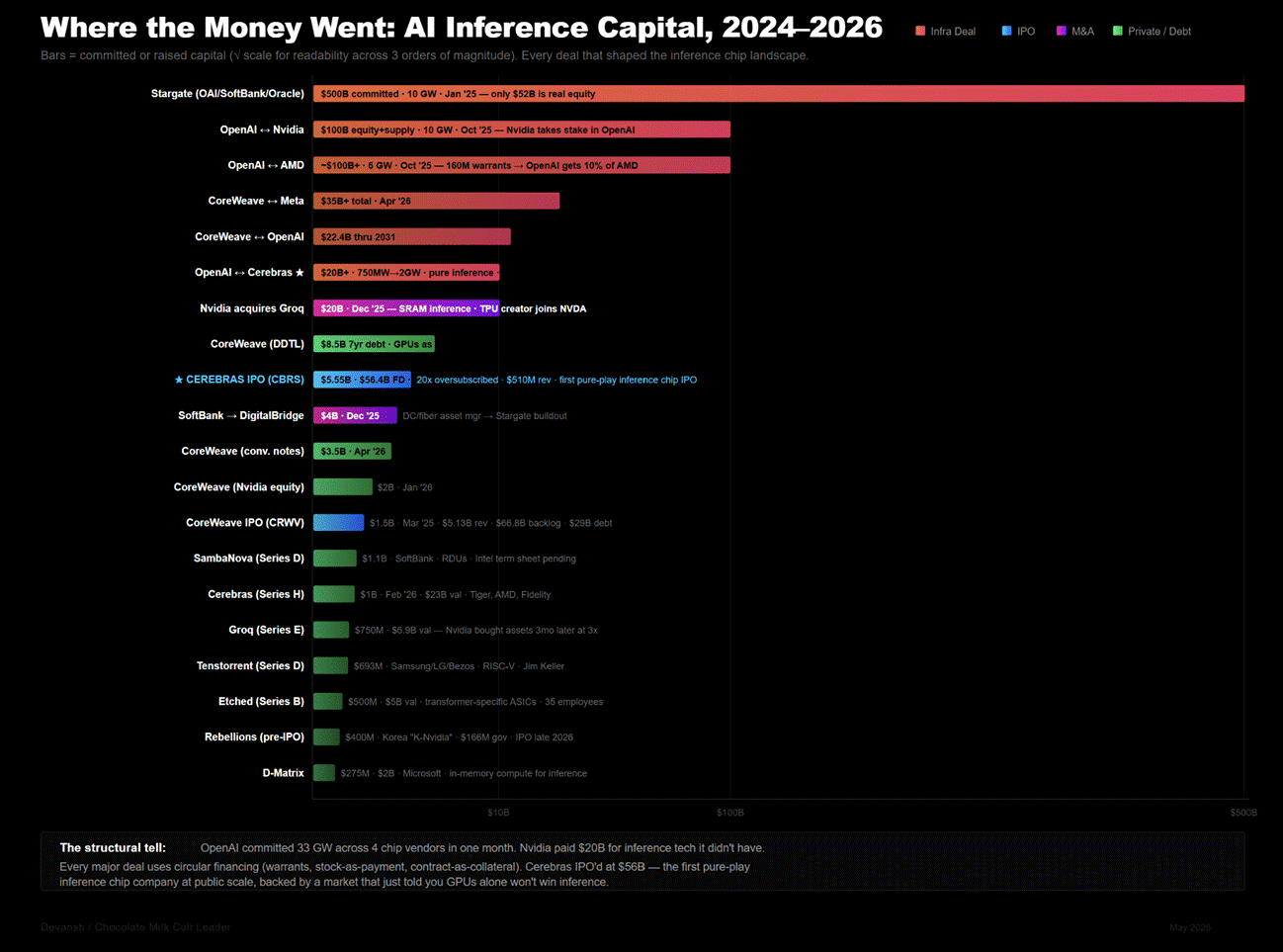
In December 2025, NVIDIA paid 20 billion dollars to acqu-hire Groq, explicitly buying its SRAM-heavy inference architecture to patch their own decoding bottleneck. Earlier this month, Cerebras (another company with a similar thesis) executed a massive initial public offering, pricing at 185 dollars a share to achieve a 66 billion dollar market capitalization. They went to market backed by a 20-billion-dollar Capacity-as-a-Service contract with OpenAI.
This is far from the only major event in the AI hardware space. Billions of dollars (trillions if you think about the plans to build Fabs) are being thrown around to address the fundamental limitations of GPUs when it comes to serving large language models at scale.
Cerebras represents one such bet against GPUs. Where GPUs spend their entire power and clock budget waiting for model weights to travel across a shared physical bus from distant memory modules, Cerebras built a chip the size of a dinner plate to physically short-circuit this memory bandwidth ceiling.
By keeping 44 gigabytes of elite SRAM permanently resident next to 900,000 active compute cores, they eliminate the off-chip round trip entirely. To drag this machine to market, they had to solve five brutal physics problems — from reticle limits to coefficient of thermal expansion mismatches — that left a forty-year graveyard of bankrupt semiconductor startups behind them.
Cerebras’s massive IPO is a clear indication of the AI industry recognizing one of it’s biggest fault lines and scrambling to find the solutions for it. However, to understand the viability of this solution, we must understand the current issue with AI Inference, why Wafer scale has historically failed, and what Cerebras is trying to do differently. This deep dive will do that by deconstructing the physical reality of wafer-scale processing against the brutal unit economics of real-world deployment. I wrote it for builders, capital allocators, and technical leaders who need to separate structural hardware moats from venture-backed marketing and ultimately make decisions on how to best engage/benefit from this massive shift in the market.
To do so, in this article, we cover:
The Bandwidth Wall: Why inference is a memory problem, and why adding GPU compute wastes silicon.
The Physics: The five physical constraints of wafer-scale manufacturing that destroyed conventional chip designs over the last forty years.
The Silicon: How Cerebras bypassed the reticle limit, power droop, and thermal expansion to manufacture a single continuous computational surface.
The Memory Math: The exact first-principles calculation behind their memory bandwidth advantage and bytes-per-FLOP scaling.
The Production Reality: The severe operational costs of unique wafer compilations, a barren software ecosystem, and unproven physical failure modes.
The Competitive Horizon: How NVIDIA’s 20-billion-dollar Groq acquisition, Google’s bifurcated TPU strategy, and the SRAM density wall dictate the survival of the architecture.
PS: I have not taken any compensation from Cerebras or anyone else for this deep dive (we have a strict independence policy). The timing of this deep dive close to their IPO is a coincidence. I started the research conversation with their team months ago, it just took me a while to really research and understand the space + I was busy with the paperwork for the o1 visa.
Executive Highlights (tl;dr of the article)
Cerebras is a bet on one claim: LLM inference is limited by memory bandwidth, not compute. During decode, GPUs have to read model weights again for each new token. The math units sit idle because the weights can’t arrive fast enough. More FLOPs don’t fix that. More bandwidth does.
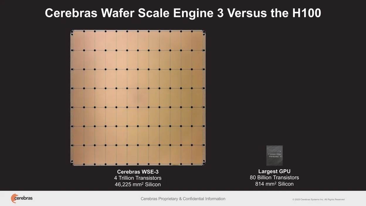
Cerebras attacks this by moving memory next to compute. Instead of cutting a wafer into separate chips, it keeps the full wafer intact and stitches the regions together. The result is a dinner-plate-sized chip with 900,000 active cores, 44 GB of on-chip SRAM, and 21 PB/s of aggregate memory bandwidth.
This was hard because wafer-scale computing breaks normal chip assumptions. A full wafer runs into five problems: lithography reticle limits, manufacturing defects, power delivery, cooling, and thermal expansion. Cerebras solves them with reticle stitching, redundant cores, compile-time routing, vertical power delivery, liquid cooling, and a connector that lets the wafer move without cracking the package.
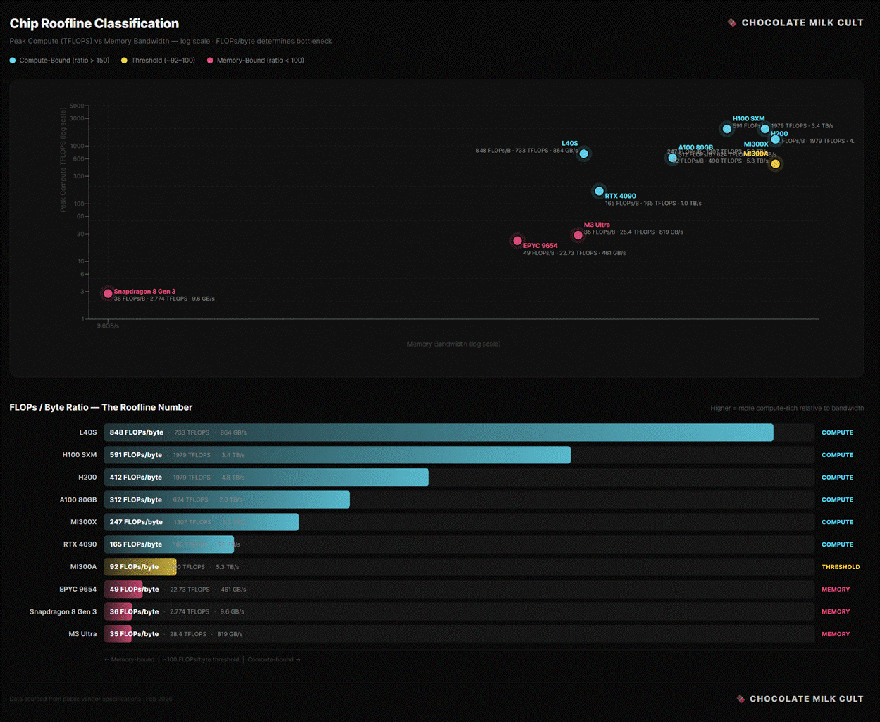
The key comparison is bytes per FLOP. WSE-3 can deliver about 0.168 bytes per FLOP. H100 delivers about 0.0034 bytes per FLOP. That gives Cerebras roughly a 50x advantage in feeding data to math units during bandwidth-bound decode. This is why its Llama 3 70B single-stream output speed can reach around 2,100 tokens/s, compared with roughly 30–50 tokens/s on a single H100.
The speed comes with a capacity problem. WSE-3 has only 44 GB of SRAM. A 70B FP16 model needs about 140 GB of weight storage, so Cerebras needs four CS-3 systems to host one full-precision instance. GPUs are slower per stream, but their HBM capacity makes large-model hosting much cheaper and simpler.
Cerebras changes serving economics. GPUs need batching because many users must share the same expensive HBM weight reads. Cerebras can run fast at Batch-1 because weights are already stored in local SRAM. But when a model spans multiple wafers, Cerebras has to keep the pipeline full with several users at once or most of the cluster sits idle.
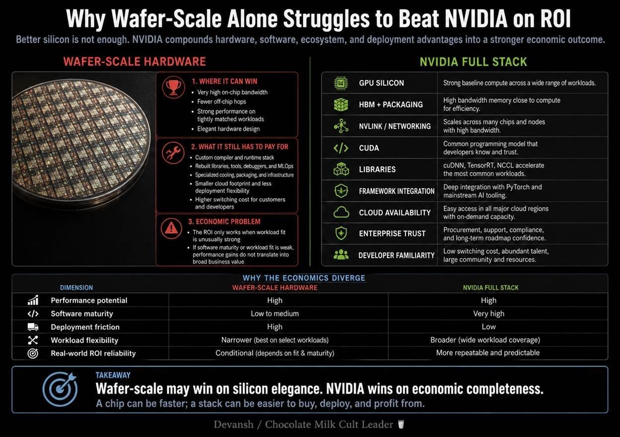
The training story is weaker. Cerebras originally targeted training by streaming weights from external MemoryX while keeping activations on wafer. The architecture made sense on paper, but frontier labs still train on NVIDIA GPUs, Google TPUs, or custom hyperscaler chips. The software ecosystem mattered more than the hardware elegance. CUDA remains the moat. Annoying little goblin. Very real.
The business case is still unproven. Cerebras has a strong physics story, but revenue concentration, the forward-looking OpenAI capacity deal, and weak baseline unit economics make the IPO story fragile. The OpenAI contract only works if Cerebras can resell idle capacity, add high-margin services, and improve system efficiency over time.
The software risk is serious. Every wafer has a unique dead-core map, so binaries are tied to specific machines. Custom compilation can take hours. Novel models may fail to compile. The CSL developer pool is tiny. The normal GPU stack — vLLM, FlashAttention, Triton, CUTLASS, xformers, HuggingFace workflows — does not carry over cleanly.
The reliability story also needs proof. A 23 kW wafer has little thermal margin. Cooling failures, voltage regulator issues, local brownouts, silent data corruption, connector fatigue, and post-deployment core failures are all real fleet-level risks. Cerebras has shown the machine can work. It has not yet shown enough public evidence that it can scale cleanly under hyperscaler operating conditions.
The final question is timing. If GPU memory systems improve fast enough, Cerebras becomes a brilliant transitional architecture. If single-stream latency becomes central to agentic AI and HBM remains the bottleneck, Cerebras sits exactly where GPUs break. The engineering is real. The advantage is measurable. The company still has to prove the market window, software stack, manufacturing scale, and unit economics all arrive before NVIDIA crushes the oxygen out of the room.
I put a lot of work into writing this newsletter. To do so, I rely on you for support. If a few more people choose to become paid subscribers, the Chocolate Milk Cult can continue to provide high-quality and accessible education and opportunities to anyone who needs it. If you think this mission is worth contributing to, please consider a premium subscription. You can do so for less than the cost of a Netflix Subscription (pay what you want here).

I provide various consulting and advisory services. If you‘d like to explore how we can work together, reach out to me through any of my socials over here or reply to this email.
Part 1: Background
Why Does LLM Decode Hit a Memory Bandwidth Wall on GPUs?
We’ve covered this idea a lot, so I’m going to breeze through this one here. If you want to understand this gap more (and how the Roofline models work), check out:
Our deep dive into Liquid AI and what makes them special for edge AI.
Our deep dive into AI inference and why its emerging as a separate category over here
An H100 executes 989 trillion floating-point operations per second. During the decode phase of large language model inference, the chip uses less than 1% of that capacity. The compute units sit idle waiting for weights to arrive from memory. Why does this happen?
Inference consists of two distinct workloads. The prefill phase processes the input prompt in parallel, generating the high arithmetic intensity (The ratio of useful math to memory traffic) that keeps a GPU busy. The decode phase generates the output sequentially. To produce one token, the chip must read essentially every weight in the model from memory, multiply those weights once, and move on. The arithmetic intensity plummets to roughly 1 FLOP per byte. At 30Gs a chip and these abysmal numbers, you’re better off paying Scale AI to whip 3rd world orphans to run the numbers manually. You might even get a Mr Beast video out of this.
This exposes the hardware’s roofline. The H100 balances compute and memory bandwidth at roughly 295 FLOPs per byte. Any workload running below that ratio is bandwidth-bound. Because decode runs at 1 FLOP per byte, it hits the memory ceiling at 1/200th of the chip’s theoretical peak. You could double the H100’s compute capacity and decode speed wouldn’t increase by a single token (this is the reason behind the memory wall we broke down here). The physical pipe between memory and compute dictates the limit.
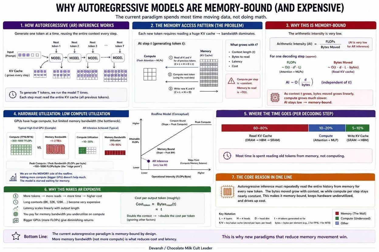
NVIDIA’s current approach is to build a wider pipe. The H100 moves 3.35 TB/s, and the B200 moves roughly 8 TB/s. But each hardware generation also scales up compute, which pushes the required balance point even higher while decode stays pinned at 1 FLOP per byte. Every additional transistor dedicated to arithmetic is wasted silicon during decode.
So what can we do here? GPUs store weights in memory stacks located millimeters away from the compute cores, connected through shared controllers. The physical alternative is to embed the memory directly adjacent to every compute core. When memory is part of the core itself, adding cores automatically scales memory bandwidth and eliminates the off-chip round trip entirely.
Sounds obvious enough, we run into a slight complication here: building a unified compute-memory architecture at scale has killed every hardware company that attempted it over the last forty years.
Let’s understand why.
Why Did Wafer-Scale Integration Fail for Forty Years?
If memory bandwidth is the bottleneck, the obvious fix is to build one massive chip where memory sits physically adjacent to every compute core. You eliminate off-chip communication entirely by weaving compute and memory across a full silicon wafer. Engineers tried this for forty years. Tried being the operative word here.
Gene Amdahl raised 230 million dollars in 1980 to build an IBM-compatible mainframe on a 2.5-inch wafer for Trilogy Systems. The fabrication technology of the era could not hit the defect densities required for a full wafer circuit. Interconnects delaminated, a prototype shorted and glowed red during a demonstration, and the company dissolved.
ETA Systems built a liquid-nitrogen-cooled wafer-scale supercomputer in 1983. The silicon worked. The ecosystem failed. Customers could not maintain the specialized nitrogen plumbing, and software development lagged behind the custom hardware.
Anamartic shipped a wafer-scale solid-state disk in 1989. The engineering functioned in production. Then commodity DRAM prices collapsed. Customers achieved the same performance by stringing together cheap DRAM modules, which destroyed the economic justification for Anamartic’s manufacturing premium.
Tesla proved modern wafer-scale packaging works with its Dojo D2 chip. They ran real training workloads on full-wafer silicon in production racks. But in April 2026, Elon Musk shut Dojo down. The chip functioned, but the narrow workload could not justify the cost of maintaining a custom software stack to compete against NVIDIA’s entrenched CUDA ecosystem.
So why does our aspiration to engage with Wafer scales keep getting Yamcha’d??
What Are the Five Physical Constraints of Wafer-Scale Silicon?
Wafer-scale computing is structurally different from conventional chip design. Playing at a bigger size means it hits five distinct physical and mathematical limits.
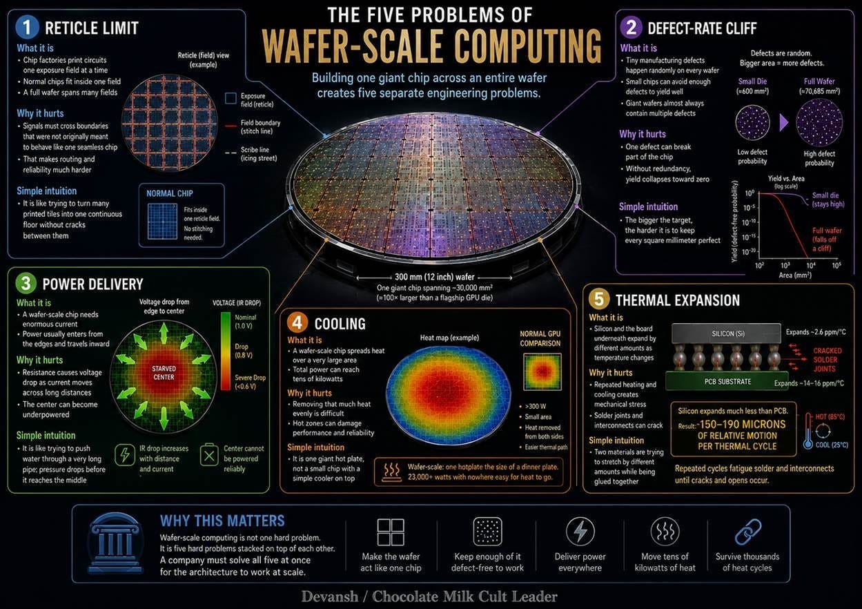
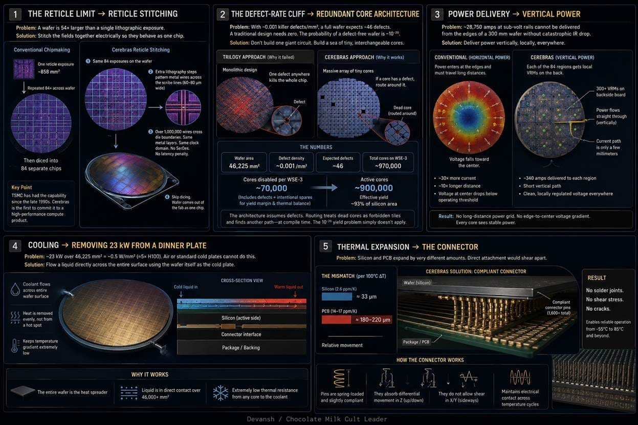
1. The Reticle Limit The Reticle Limit is a fundamental problem for wafer-scale integration because the lithography process can only expose a maximum area of about 858 square millimeters per shot, meaning a full 300-millimeter wafer requires 54 separate reticle fields. For the wafer to function as a single, unified chip, electrical connections must be routed across the boundaries between these fields. However, these boundaries are the “scribe lines,” which are strictly designed for physical cutting (dicing) and not for carrying electrical signals. This means the standard process creates discontinuities across the wafer where a unified electrical path is required, making a single functional chip mathematically impossible without a specialized technique like reticle stitching.
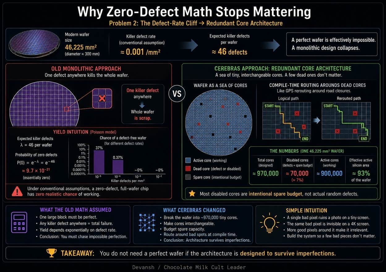
2. The Defect-Rate Cliff Mature semiconductor manufacturing produces roughly 0.001 killer defects per square millimeter. For a standard 814-square-millimeter die, the Poisson probability allows for 60 to 80 percent yields. Scale that math to a 46,225-square-millimeter wafer, and the probability of a completely defect-free wafer drops to 10^-20. In conventional design, a single defect kills the entire die. Without a mechanism to dynamically route around dead silicon, a functioning wafer-scale chip is mathematically impossible.
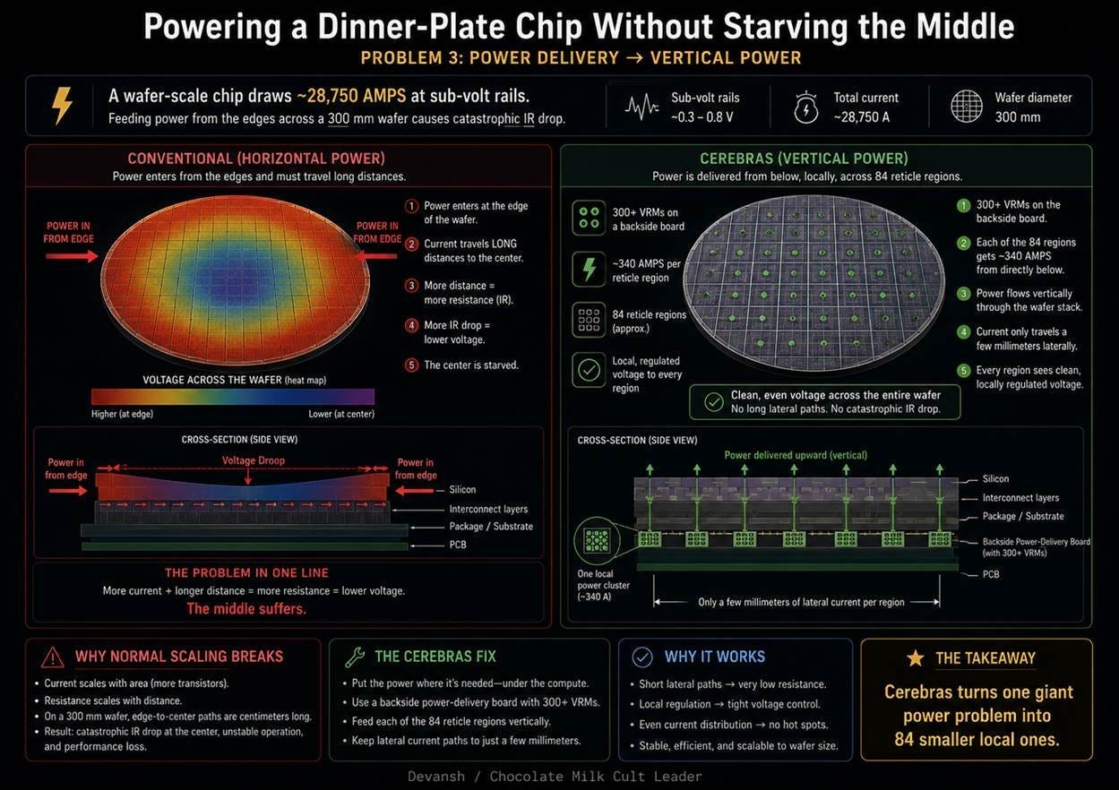
3. Power Delivery A wafer-scale chip at full load draws roughly 28,750 amps at sub-volt levels. You cannot push that much current horizontally across 300 millimeters of silicon b/c the voltage drops as it travels — a physical phenomenon known as IR drop. By the time the current reaches the interior of the wafer, the voltage sags too low for the cores to operate. You cannot power a wafer from its edges like a standard chip.
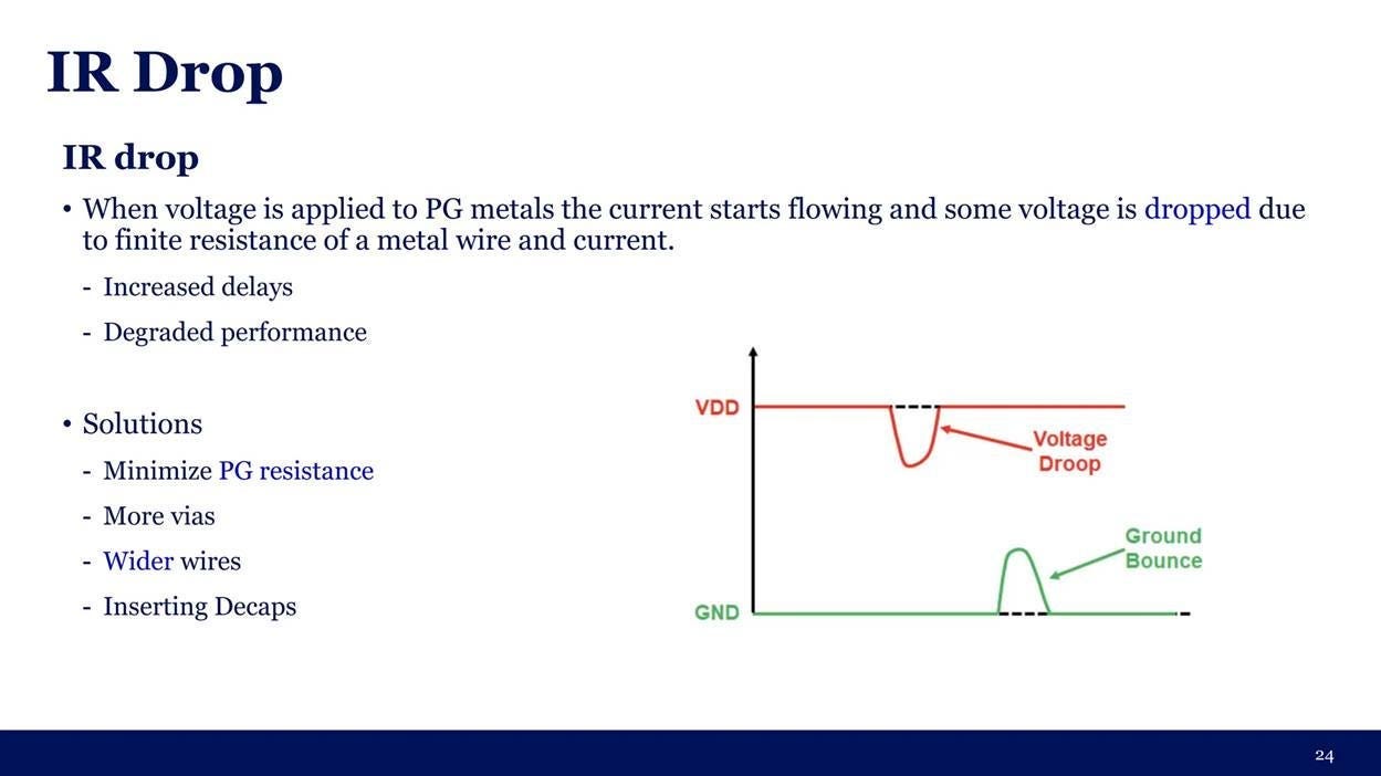
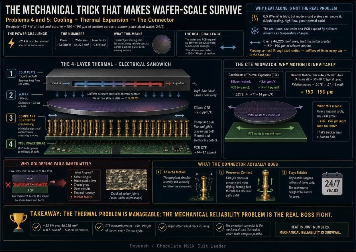
4. Cooling A modern wafer-scale chip dissipates roughly 23 kilowatts across 46,225 square millimeters. That creates a heat flux of 0.5 watts per square millimeter — five times the thermal density of an H100. Conventional air cooling cannot move this much heat. Standard liquid cold plates also fail because the heat spreads uniformly across an area the size of a dinner plate rather than concentrating in a small GPU footprint.
5. Thermal Expansion Silicon has a coefficient of thermal expansion (CTE) of 2.6 parts per million per Kelvin. Standard printed circuit board (PCB) material expands at 14 to 17 parts per million per Kelvin. Across a 215-millimeter span with a 60-degree Celsius temperature swing, the silicon expands 33 microns while the PCB expands roughly 200 microns. Every thermal cycle, the board and the wafer try to slide against each other by nearly a fifth of a millimeter. This relative motion shears standard solder joints apart on the first cycle. It is a physical hard stop for standard packaging.
So Why Does Cerebras Exist?
Given all these challenges we’ve been discussing, you might be wondering what kind of people decide to dedicate themselves to wafer-scale chips in our present age. If the generations of Arsenal fans have taught us anything, humanity’s delusion and hubris are inexhaustible commodities. So the founders of Cerebras looked at all the challenges and said “Nah, I’d win”.
Cerebras formed in 2016 around the core team from SeaMicro, a low-power server startup acquired and later shut down by AMD. They realized early that the industry’s default scaling method — adding more boxes and connecting them — was hitting a power and cost wall. The interconnect itself was becoming the bottleneck.
Now that we have the background, let’s look at how our Cere-bros have set out to solve the reticle limit, defect tolerance, power delivery, cooling, and thermal expansion simultaneously on the same wafer at volume.

Part 2: How Cerebras Builds a Chip the Size of a Dinner Plate
Building a commercially viable chip required solving all 5 problems together. Let’s see how this is accomplished.
1. The Reticle Limit and the Dicing Step
Lithography optics can only print 858 square millimeters of silicon per exposure. Foundries normally print a pattern 84 times across a wafer and use a saw to cut the silicon into 84 independent chips. Cerebras alters this process. They use standard equipment to print the 84 patterns, but then add lithography steps to print over one million microscopic metal wires directly across the “scribe lines” where the saw would normally cut.
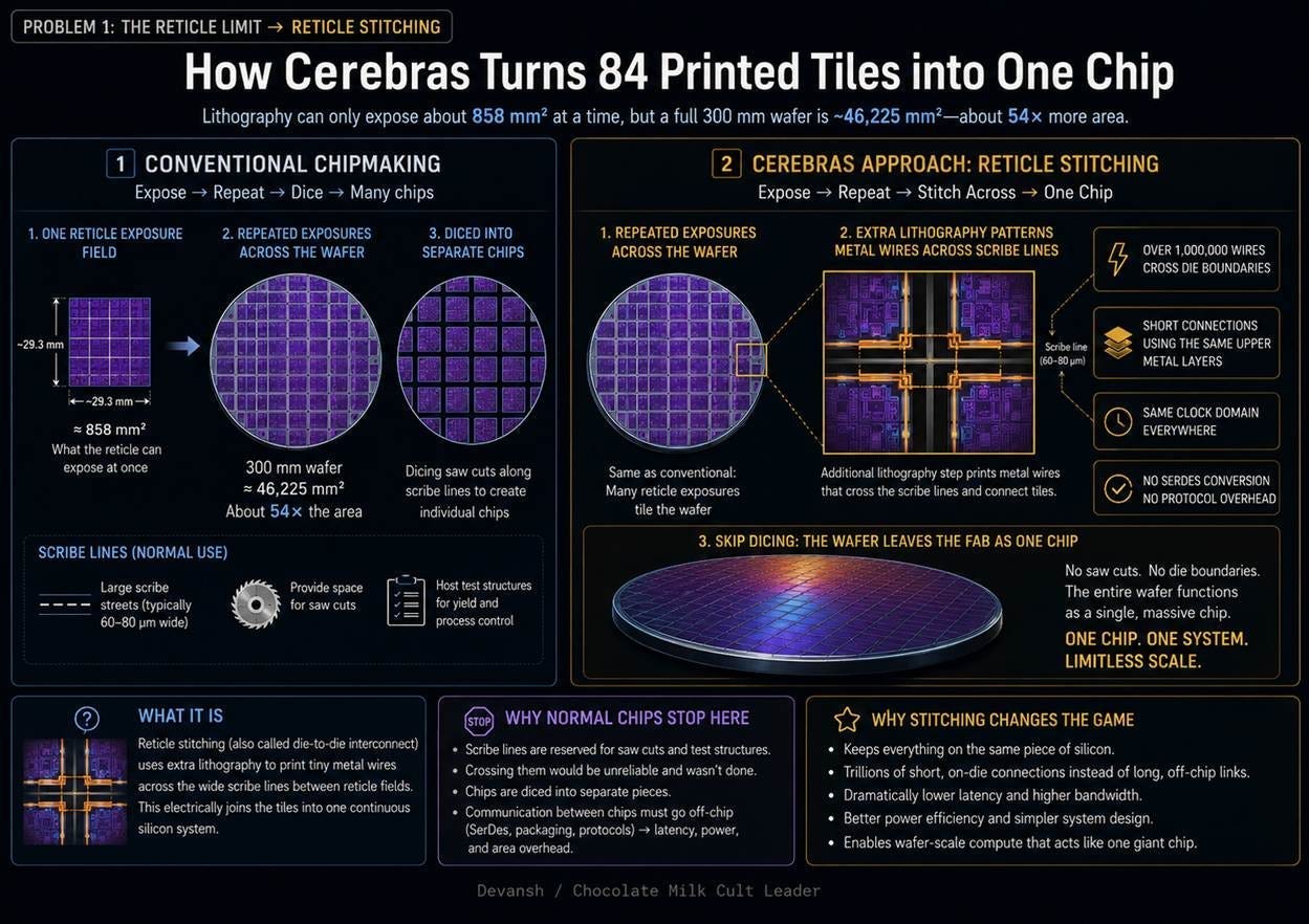
Cerebras simply skips the dicing step. This is the foundation of the architecture. By leaving the wafer intact, they preserve those one million wires. This transforms 84 separate chips into a single continuous computational surface. Data never leaves the silicon to travel between regions. This eliminates the massive latency, bandwidth bottlenecks, and power penalties required to send signals across standard copper cables or optical switches (this is one of the reasons that photonics has popped off too; they use photons to do math, which is a very cool idea, will do a deep dive into the viability of it sometime).
2. The Defect-Rate Cliff and Redundant Cores
Previous wafer-scale attempts failed because they built monolithic circuits. A monolithic circuit acts like a single mechanical watch; if one microscopic gear has a manufacturing defect, the entire watch stops. Mature fabrication guarantees roughly 46 defects per wafer. Under standard design rules, a functioning wafer-scale chip is mathematically impossible.
Cerebras abandoned the monolithic approach. They built the wafer as a grid of roughly 970,000 completely independent computational cores. This way, if a manufacturing defect strikes a core, only that specific core dies. The surrounding cores continue operating. The Cerebras compiler maps the location of dead cores and routes data around them at compile time, exactly like a GPS routing traffic around a closed road. Cerebras intentionally budgets for 70,000 disabled cores to absorb the 46 expected manufacturing defects (budgeting several orders of magnitude higher is smart given the complexity of their build and the relative unfamiliarity the ecosystem has with their stuff). This architecture converts a fatal yield problem into a manageable routing exercise, achieving 93 percent active silicon.
3. Power Delivery and the Horizontal Bottleneck
A wafer-scale chip draws 28,750 amps at sub-volt levels under full load. Conventional chips route power horizontally from the package edges inward. However, metal wiring naturally resists electrical current. This resistance causes the voltage to drop as it travels — a phenomenon known as IR drop. On a standard chip, the horizontal distance is short and the voltage drop is harmless. On a massive 300-millimeter wafer, pushing power horizontally from the edges would starve the interior cores since they would receive too little voltage to turn on.
Cerebras bypassed the horizontal bottleneck entirely by delivering power vertically. A dedicated circuit board sits directly behind the wafer. It pushes current perpendicularly into the back of the silicon through hundreds of local voltage regulators. Current travels only millimeters to reach any given core. Every region receives direct, clean power regardless of its location on the wafer.
4 & 5. Thermal Expansion and the Floating Connector
The WSE-3 generates 23 kilowatts of heat. Modern liquid cold plates can easily extract this heat. The actual barrier is mechanical expansion. Silicon and printed circuit boards (PCBs) expand at different rates when heated. Across a massive 215-millimeter span, this difference compounds. During a normal thermal cycle, the circuit board expands nearly a fifth of a millimeter further than the silicon wafer. If you soldered the wafer directly to the board, this sliding motion would shear the metal joints completely off on the first cycle.
Cerebras solved this by refusing to solder the wafer. The wafer floats. A proprietary mechanical connector sits between the bare silicon and the underlying circuit board. This connector acts as a microscopic suspension system. It bends, flexes, and compresses to absorb the differing thermal expansion while maintaining continuous electrical contact for power and data.
What Is Inside Each Core?
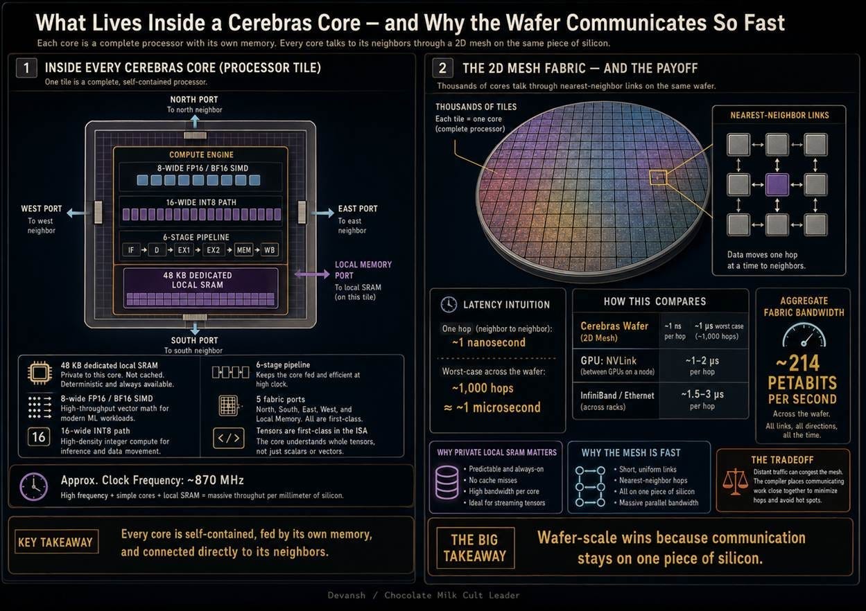
With the wafer-scale physics solved, Cerebras packed the silicon with 900,000 active processor tiles. Each core is tiny — about 0.05 square millimeters. But the most important architectural decisions aren’t about the size of the core; they are about what Cerebras stripped away from standard GPU design.
How Cerebras Handles Memory
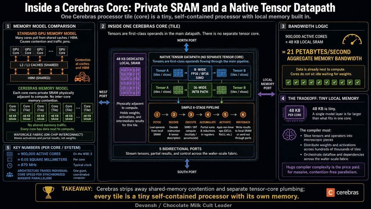
On a standard GPU, memory is a centralized pool. Thousands of compute cores pull data from off-chip High Bandwidth Memory (HBM) or shared internal caches. This creates a traffic jam since cores fight for bandwidth and wait in line for their data to arrive through complex memory controllers.
Cerebras abandons shared memory entirely. Inside each of the 900,000 cores sits 48 kilobytes of dedicated Static Random-Access Memory (SRAM). Cores do not share this memory, and no other core contends for it. Because memory physically touches the compute units, aggregate bandwidth scales linearly with every core added. This is how the WSE-3 hits 21 petabytes per second of memory bandwidth — thousands of times more than a GPU. The compute units never sit idle waiting for weights to arrive.
There is an important tradeoff here: 48 kilobytes is incredibly small. A GPU can load a massive, gigabyte-sized matrix into shared memory for all cores to access simultaneously, but Cerebras cannot. To make this work, the compiler must surgically slice neural networks into microscopic pieces and distribute the weights across hundreds of thousands of independent memory vaults. There is a lot of general life wisdom in how the hardware team successfully bypassed a massive problem (the physical memory wall) by offloading 100% of the psychological trauma to the software engineers. Bois, take notes.
How Cerebras Handles the Datapath
Modern GPUs use “scalar” units for standard math and specialized “tensor cores” built specifically to smash matrices together. Constantly moving data between these separate units consumes time and power.
Cerebras, on the other hand, treats tensors as first-class operands within the instruction set. There is no separate tensor core. Each core executes eight 16-bit floating-point operations per cycle through a simple six-stage pipeline. The cores run at approximately 870 megahertz, which is roughly half the clock speed of an H100. The architecture happily trades the sheer speed of an individual core for the overwhelming, synchronized parallelism of 900,000 cores working simultaneously.
The Fabric: How Cerebras Kills the Network-on-Chip
To manage communication, standard processors rely on a “Network-on-Chip” — a dedicated layer of hardware routers and buses built into the silicon just to manage traffic. This creates a problem: If data needs to leave the chip entirely to reach another GPU, the toll skyrockets. It must exit the die, cross a circuit board, convert into optical signals, hit an external switch, and travel down an InfiniBand or NVLink cable. Every boundary adds latency, protocol overhead, and a bandwidth bottleneck.
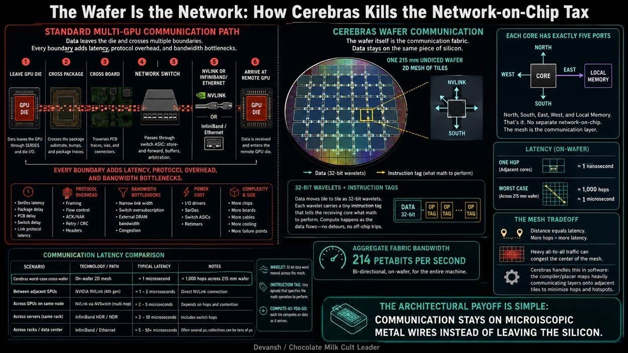
Cerebras eliminated the Network-on-Chip entirely. Because the wafer is never diced, data never has to leave the silicon. Every core has exactly five physical connection ports. Four connect directly to its immediate neighbors, and the fifth connects to its local memory. The two-dimensional grid of compute cores is the communication layer. Data travels seamlessly across the silicon as 32-bit “wavelets,” carrying tiny instruction tags that tell the receiving core exactly what math to perform as the data passes through.
Think about how fast this makes your operations. A single hop between adjacent cores takes roughly one nanosecond. Crossing the entire 215-millimeter wafer — roughly 1,000 hops — takes about one microsecond. That worst-case latency on a Cerebras wafer matches the best-case latency between two adjacent GPUs connected by NVLink in a server rack. Because communication requires only microscopic metal wires rather than optical cables, the internal fabric provides 214 petabits per second of bandwidth.
However, a two-dimensional mesh has a structural weakness: distance equals latency, and intersecting traffic causes congestion. If cores on opposite sides of the wafer constantly talk to each other, the center of the grid jams. Cerebras handles this entirely in software. The compiler is forced to be aggressively intelligent, mapping the neural network spatially so that layers requiring heavy communication are placed on physically adjacent silicon tiles.
All of this is incredibly sophisticated, and we should really take a step back and appreciate the engineering that makes this possible. As I mentioned earlier, it took me about a 1–2 months of on and off research to even get to a functional understanding of Cerebras and what it does. However, just as Pep’s ability to overthink tactics against Burnley can sometimes cause him to bench Rodri to play Gundogan deeper (???? it’s been years, and I’m still so fucking confused by that shit), intricate engineering can be a challenge to scale well. And this might have already started to show up with Cerebras.
Three Generations and the SRAM Density Wall
The physical limits of this architecture are beginning to show in its generational scaling.
The first WSE shipped in 2019 with 400,000 cores, proving that the wafer-scale physics problems had commercial solutions. The WSE-2 shipped in 2021, proving the architecture could scale by doubling both core count and memory capacity.
The WSE-3 shipped in 2024 and hit a wall. Compared to the previous generation, core count grew only 6 percent and SRAM capacity grew only 10 percent (tbf, raw compute capacity exploded 17-fold to 125 petaflops so maybe I’m tripping out over nothing).
This imbalance exposes the “SRAM density wall” plaguing the entire semiconductor industry. The WSE-3 uses TSMC’s 5-nanometer process. As fabrication nodes shrink, standard logic transistors scale down beautifully. SRAM memory cells do not. They require six carefully balanced transistors just to hold a single bit of data, and they hit a physical floor where shrinking them further compromises their electrical stability. Wall Street is currently modeling software-like margin expansions through 2030 for these hardware companies. Its going to very interesting to see how their spreadsheet merchants try to adjust their discounted cash flow models for quantum tunneling.
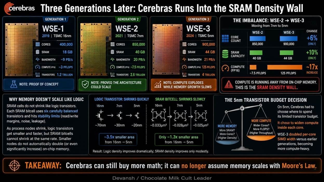
Because Cerebras relies entirely on embedded SRAM rather than external memory modules, they are highly exposed to this limitation. Forced to choose how to spend their 5-nanometer silicon budget, Cerebras couldn’t double the memory or the core count. Instead, they spent their transistor budget inside the core, widening the compute datapaths to massively increase mathematical throughput. I’m not a semis guys so I’m not going to make any strong claims about this, but this did seem like a possible trend to monitor. Now I might be turning windmills into giants here, but I think that any analyst trying to price the future of this company should be looking at how the Cerebros (and the rest of this industry) tackle this problem and its various siblings.
For now, let’s get back to our analysis of the present by understanding the insane performance numbers that have underpinned Cerebras’s amazing IPO.
Part 3: How Good is Cerebras Really?
The architectural argument hinges on a single claim: moving memory directly adjacent to compute cores eliminates the bandwidth bottleneck. To evaluate this honestly, the claims must be translated into first-principles mathematics and measured against observed production benchmarks.
Deriving the 21 PB/s Number
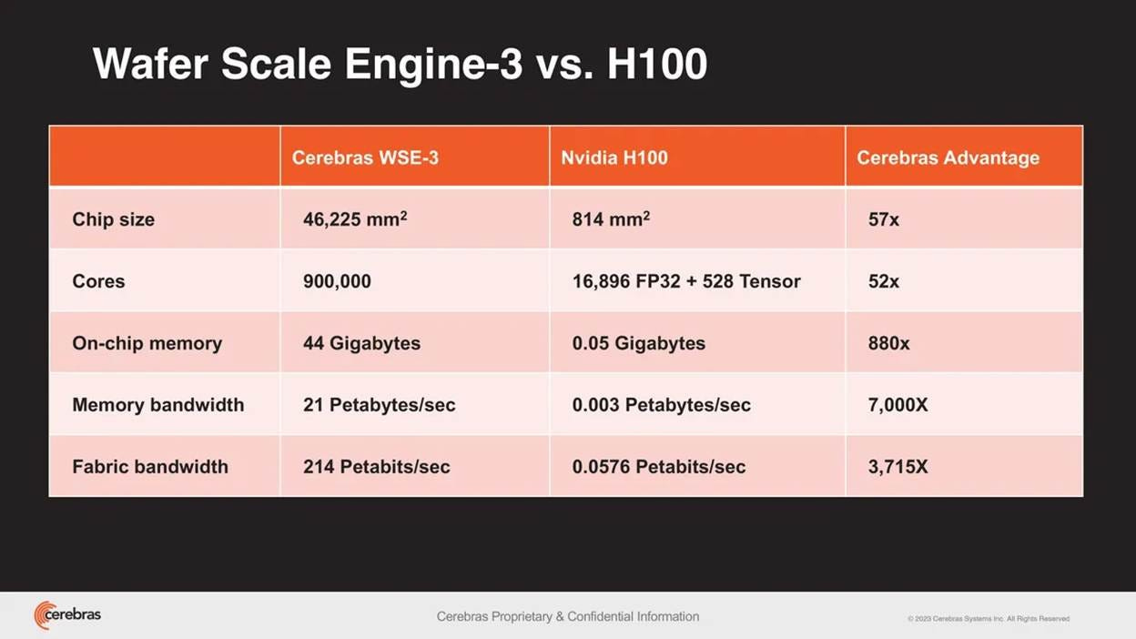
Cerebras’s headline specification — 21 petabits per second (PB/s) of memory bandwidth — presents an apparent 6,272-fold advantage over an NVIDIA H100’s 3.35 terabytes per second (TB/s).
Normally, when we see such large deltas, it’s fair to have some skepticism. However, this aggregate figure is real, but it measures a completely different physical architecture than a GPU’s shared memory system.
Each of the 900,000 active cores on the WSE-3 has 48 kilobytes (KB) of private, dedicated local SRAM. Operating at a clock speed of approximately 870 megahertz (MHz) with a datapath width of 24 bytes per read, a single core can pull data from its private SRAM at roughly 23 gigabytes per second (GB/s). Multiplying this private, contention-free performance across all 900,000 active ports running in parallel yields the aggregate figure:
900,000 cores multiplied by 23.3 GB/s equals approximately 21 PB/s
This massive number represents the sum total of 900,000 independent, simultaneous memory transfers. It does not describe a single centralized memory pool flowing through a massive wire.
By contrast, the H100’s 3.35 TB/s describes a single, shared ceiling. All 132 streaming multiprocessors (SMs) must compete for access to the same High Bandwidth Memory (HBM) modules through a shared memory bus. When one SM reads a model weight, it consumes a portion of that fixed bandwidth pool, creating structural contention that reduces effective per-core throughput under real workloads. On the WSE-3, Core #47 reading its local SRAM has zero physical impact on Core #48’s ability to read its own memory at full speed. Because bandwidth is simply the measurement of how much data can flow from memory to the compute units in a given second, giving every core its own memory port means the system’s total bandwidth is just the sum of all cores operating at once. This allows the architecture’s data delivery to scale linearly without a shared physical bus to bottleneck traffic.
But given that these are different operations, how do we make an apples-to-apples comparison for this operation?
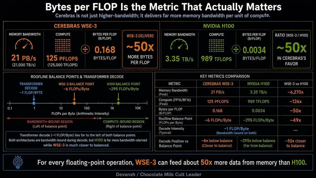
The Balance Metric: Bytes per FLOP
To understand how effectively these chips can actually use their raw performance, we have to evaluate their architectural balance. We do this by dividing memory bandwidth (the numerator) by peak floating-point operations per second (the denominator). The numerator tells us how fast the chip can fetch data from memory, while the denominator tells us how fast the chip’s arithmetic units can process that data. The resulting bytes-per-FLOP ratio defines exactly how many bytes of data the hardware can deliver for every single mathematical operation it performs, revealing whether the chip is starving for data.
WSE-3: 21 PB/s divided by 125 PFLOPS peak compute equals 0.168 bytes per FLOP.
H100: 3.35 TB/s divided by 989 TFLOPS peak compute equals 0.0034 bytes per FLOP.
This reveals a 50-fold structural advantage for Cerebras. For every floating-point operation executed, the Cerebras architecture can deliver 50 times more data to its arithmetic units than an H100.
Sheesh. Do you think now would be a good time to apply for a job with them? To my low-tech Indian mom, the terms “I convince tech companies to invest in open source research” and “I’m a glorified beggar” are dangerously similar.
During the sequential decode phase of an LLM, the chip is starved for data because it only performs roughly 1 FLOP of math for every byte of weights it reads. The H100’s physical balance point requires a massive 295 FLOPs of math per byte to keep its transistors busy, pinning it at 1/295th of its peak capacity during decode. Because the WSE-3 feeds its units 50 times more data per operation, its balance point sits at roughly 6 FLOPs per byte, allowing it to operate at 1/6th of its compute peak.
Benchmark Verification against Production Reality
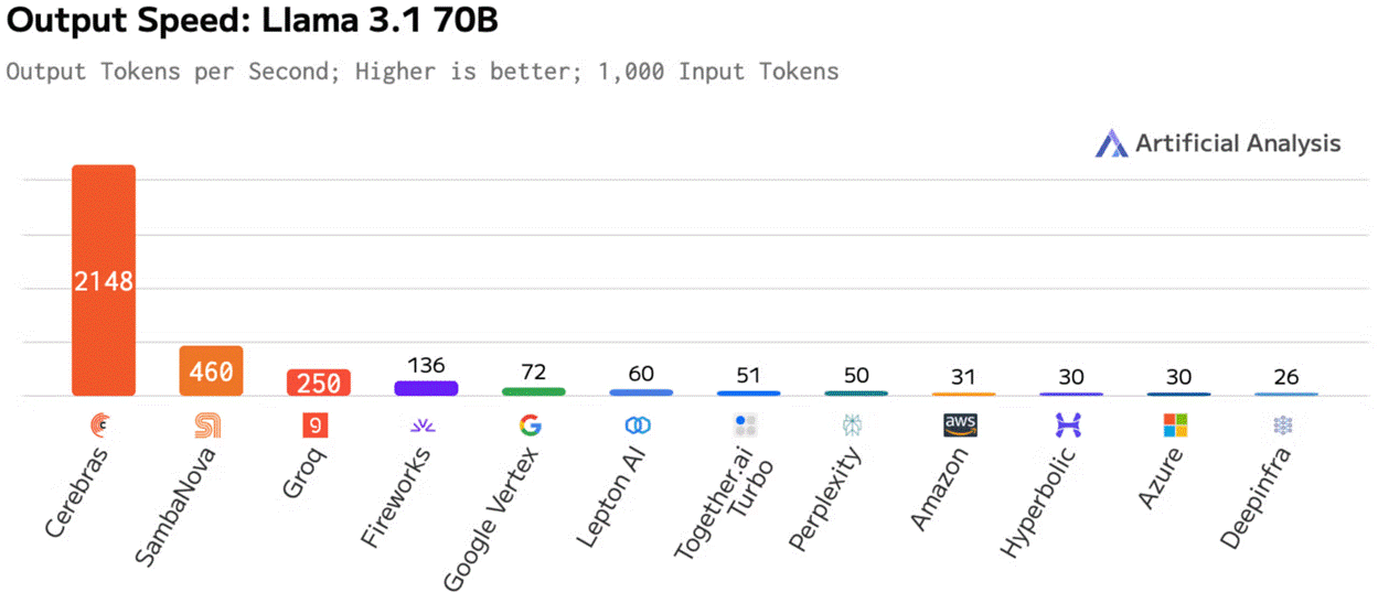
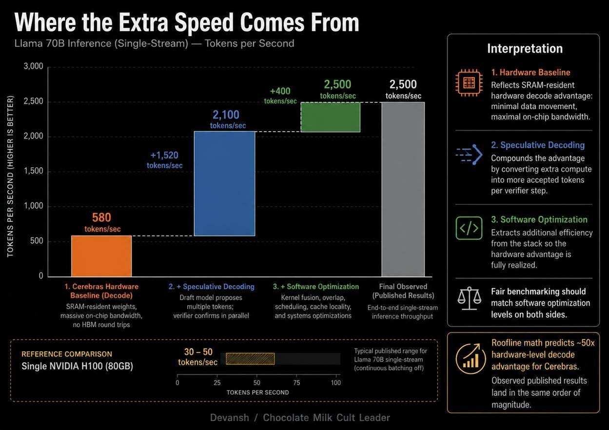
This roofline model predicts that a bandwidth-bound model should decode roughly 50 times faster per stream on the WSE-3 than on an H100. Production benchmarks validate this physical reality: a Llama-3 70B parameter model achieves a single-stream decode speed of roughly 2,100 tokens per second on Cerebras, compared to 30 to 50 tokens per second on a single H100.
This speedup confirms that the performance delta is driven by weight-reading latency, not raw math throughput.
Given how important inference is to their company, it makes sense to understand how Cerebras handles inference.
How LLM Inference Physically Operates on Wafer-Scale Silicon
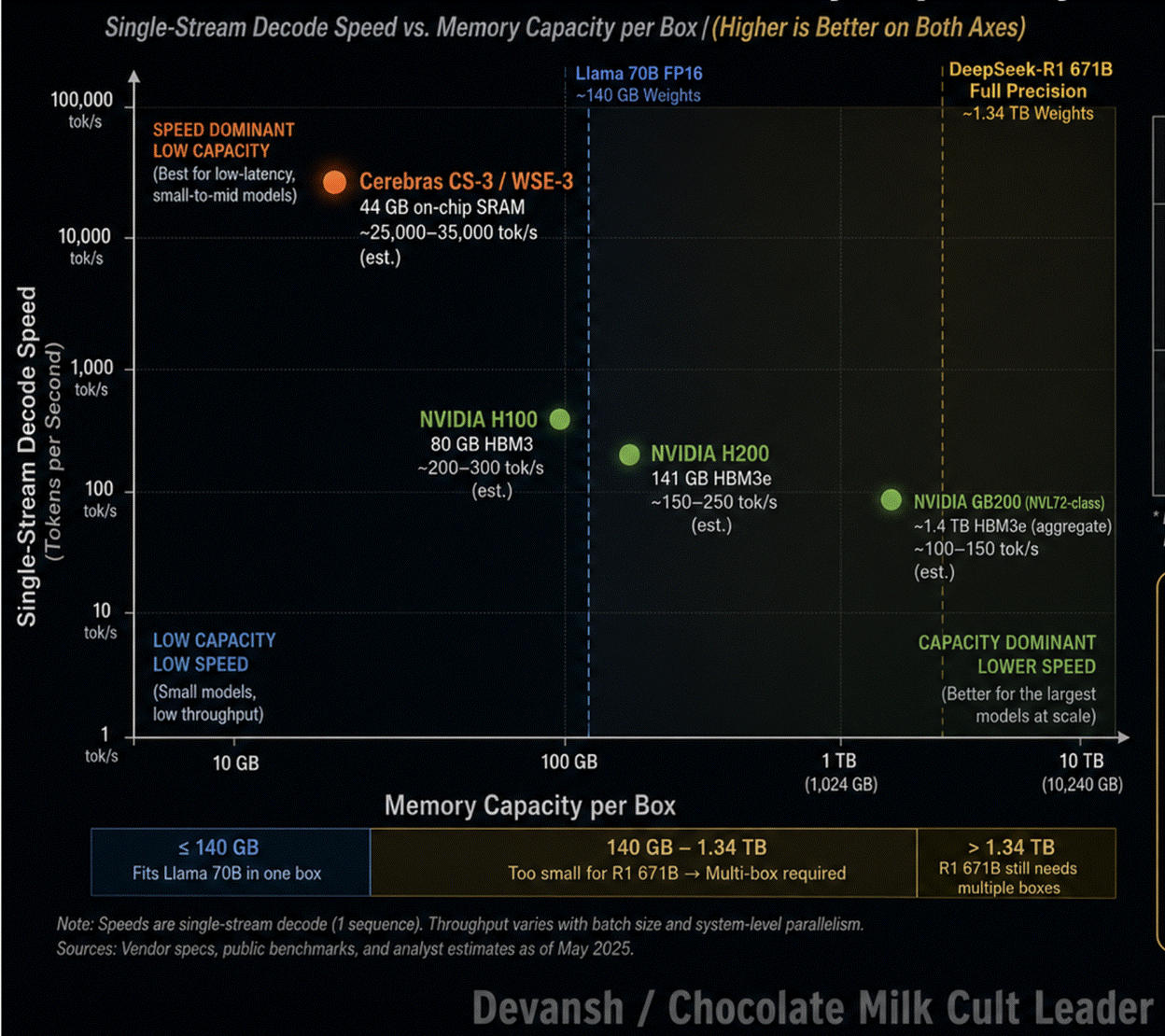
Serving a model like Llama-3 70B at FP16 precision requires roughly 140 gigabytes (GB) of weight storage. Because a single WSE-3 contains only 44 GB of local SRAM, the model cannot fit on one wafer. Cerebras chains four CS-3 systems together, creating 176 GB of aggregate on-chip SRAM, leaving 36 GB of headroom for activations and the Key-Value (KV) cache.
The model’s 80 transformer layer boundaries split evenly across the cluster, allocating roughly 20 layers per wafer. This creates pipeline parallelism at the layer boundaries:
MemoryX cold-loads the permanent weight shards into each wafer’s local SRAM, then goes silent.
During inference, a single user token enters Wafer 1 and processes sequentially through layers 1 to 20.
Wafer 1 transmits the resulting output activations to Wafer 2 via an external Ethernet interconnect.
Wafer 2 processes layers 21 to 40 using its own SRAM-resident weights, passing subsequent activations down the chain until the token exits Wafer 4.
At no point during active generation does any core make an off-chip round trip to fetch a model weight. Every weight read is a local, zero-contention SRAM access operating at full speed.
This physical layout upends traditional GPU serving economics. On a GPU, inference providers must stack multiple user requests into large batches (e.g., Batch-8 or Batch-64). This amortizes the bandwidth cost: reading a weight once from HBM allows it to be reused across multiple independent user tokens, inflating the arithmetic intensity to keep the compute units busy. GPU profitability depends on accumulation.
On Cerebras, because the weights are locked inside the local SRAM of each core, there is no shared memory bus to amortize. A single user runs at Batch-1 — commanding the entire local bandwidth of their dedicated core cluster — and still hits the peak 2,100 tokens per second. Bandwidth is not a shared resource; every user achieves maximum per-stream velocity because no concurrent streams compete for memory access.
How Cerebras Resolves the Pipeline Bubble
Pipeline parallelism at Batch-1 introduces a severe structural flaw: if a single token flows sequentially through four distinct wafers, then three out of the four wafers are completely idle at any given millisecond. Left unmanaged, 75 percent of the cluster’s silicon sits dark, completely erasing the wafer-scale performance premium.
Cerebras resolves this by filling the physical pipeline with independent user streams, replicating traditional hardware pipelining at a macro level. In steady state, the system processes four concurrent users simultaneously:
Wafer 1 processes Layer 1–20 activations for User D.
Wafer 2 processes Layer 21–40 activations for User C.
Wafer 3 processes Layer 41–60 activations for User B.
Wafer 4 processes Layer 61–80 activations for User A.
As Wafer 4 finishes User A’s token and emits it to the user, User A’s next token enters Wafer 1 behind User D. This scheduling optimization fills the pipeline, pushing hardware utilization close to 100 percent without sacrificing individual per-stream speeds. The system achieves efficiency at small, tightly bounded batch sizes (4 to 10 concurrent users) rather than the massive concurrent batches of hundreds required by GPU continuous-batching frameworks.
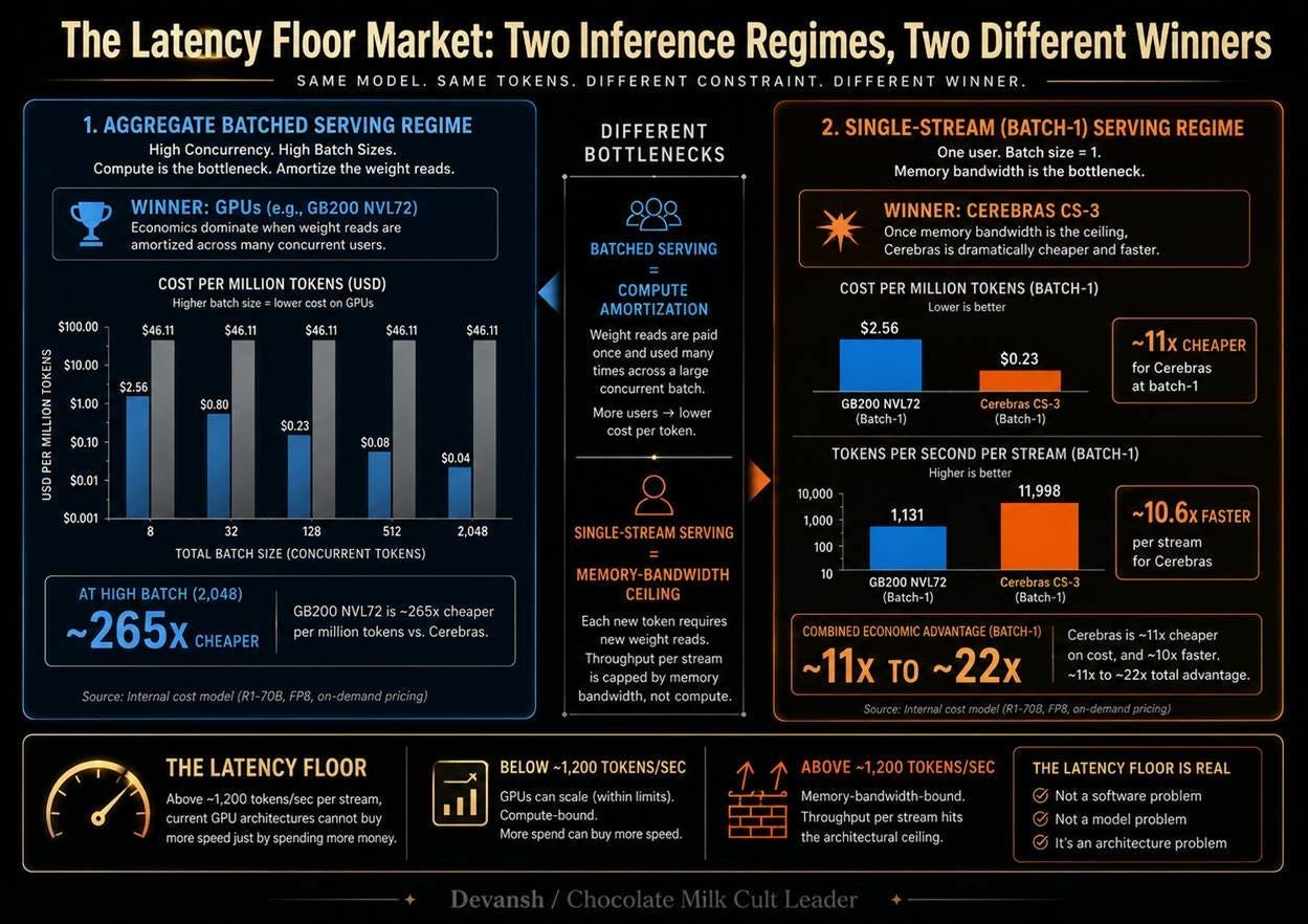
Cerebras does not compete with NVIDIA on high-density commodity throughput. Its addressable commercial market is strictly bounded by the latency floor: applications where per-stream execution speeds must exceed the physical capabilities of an HBM bus. Everything below that floor belongs exclusively to the GPU ecosystem.
The Training Moat and why Cerebras Pivoted to Inference
The WSE architecture was originally designed for AI training, which requires an inversion of the GPU memory model.
On a GPU, model weights must remain resident in HBM during training because a backward pass requires immediate, sequential access to read weights, calculate activations, compute gradients, and execute weight updates for a given layer. The data and intermediate activations are what stream through the hardware.
On Cerebras, the 44 GB on-chip SRAM is too small to hold giant training states but large enough to hold all activations for a single layer. The paradigm flips: activations are kept resident in SRAM, while model weights stream into the wafer from the external MemoryX subsystem one layer at a time. The wafer loads Layer 1’s weights, computes the output activations, updates the activation state on-chip, discards Layer 1’s weights, and loads Layer 2’s weights from the external pool. For multi-wafer training scales, an external fabric called SwarmX broadcasts these weights across systems and reduces the resulting gradients.
This decoupling means model sizes can scale without a hard physical ceiling, as weights are stored externally and streamed through the wafer. In principle, an arbitrarily large model can be trained on a fixed slice of wafer hardware.
In practice, zero frontier labs utilize Cerebras for training. OpenAI, Anthropic, Google, Meta, and xAI train exclusively on NVIDIA GPUs, Google TPUs, or custom hyperscaler silicon. The weight-streaming training model failed to achieve commercial adoption due to the sheer gravitational pull of the existing software ecosystem. CUDA, PyTorch’s native GPU backends, and an industry-wide library of optimized human kernels created a software moat that a raw hardware memory advantage could not breach. It is a brutal lesson in hardware engineering: you can successfully rewrite the physical boundaries of semiconductor memory, but you cannot convince a machine learning researcher to learn a new API.
Cerebras’s commercial survival was dictated by the shifting economics of production inference. The same SRAM bandwidth profile that was a secondary consideration during training became a decisive bottleneck during sequential LLM decode. The company’s strategic pivot to inference was a forced entry into the only market segment where their architecture’s physics mapped directly to the industry’s primary cost center.
However, there is a blocker that Cerebras will have to address if it is to move forward on capitalizing on this shift.
The Capacity Deficit: What the Cerebras Architecture Gives Up
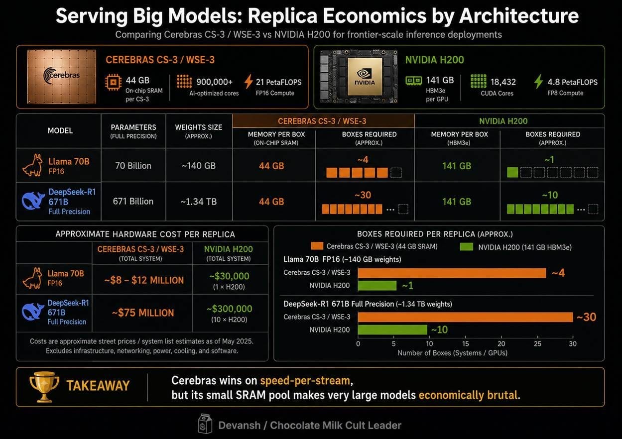
The severe tradeoff of choosing 44 GB of elite on-chip SRAM over 141 GB of commodity HBM is a devastating capacity deficit that hits large-scale frontier models immediately.
Serving a standard Llama-3 70B model at full precision requires four interconnected CS-3 systems, representing an infrastructure cost of 8 to 12 million dollars to host a single model instance. A single NVIDIA H200 or B200 GPU chip, carrying up to 141 GB of high-capacity HBM, can house that entire 70B parameter model on a single 30,000-dollar card. The GPU delivers significantly lower per-stream token speed, but at a capital footprint that is orders of magnitude smaller.
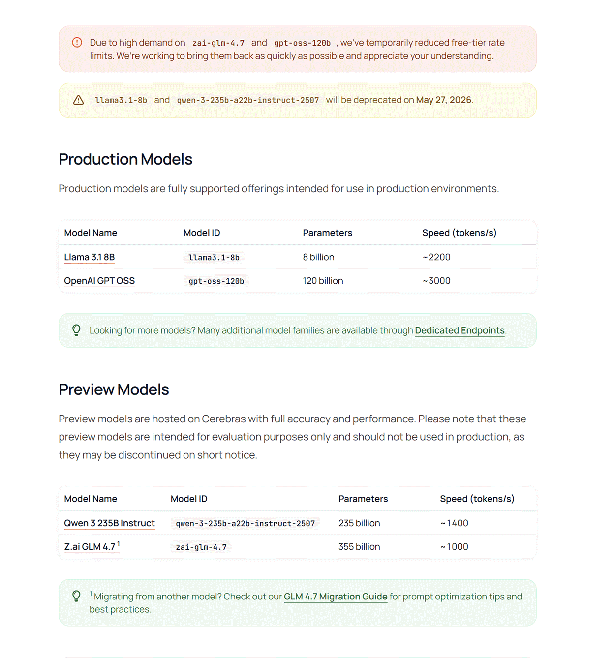
This constraint becomes fatal when scaled to massive mixture-of-experts models. Serving DeepSeek-R1 (671 billion parameters) at full precision would require a minimum cluster of 30 connected CS-3 systems — a raw hardware outlay of roughly 75 million dollars per model replica. Consequently, Cerebras cannot practically host or serve the largest, highest-volume open-weights model in the current market. As a direct result of this physical capacity floor, Cerebras’s live inference catalog remains constrained to just four models, two of which are scheduled for complete deprecation on May 27, 2026. However, the rise of attention given to edge models (which are the best types of models for Cerebras), might provide the perfect outlet to Cerebras.
The OpenAI Capacity-as-A-Service Contract
To survive outside its primary sovereign revenue base — where Abu Dhabi entities accounted for 86 percent of 2025 recognized revenue — Cerebras executed a massive Master Revenue Agreement with OpenAI in December 2025. The headline terms outline an infrastructure allocation of 750 megawatts (MW) of datacenter capacity from 2026 to 2028, expandable to 2 gigawatts (GW) by 2030, valued at a gross contract potential exceeding 20 billion dollars.
The underlying unit economics of this agreement reveal that the contract operates as a loss-leader to justify the capital buildout. The contract prices out to approximately 9 million dollars per megawatt per year. Based on the active power profile of the CS-3, this yields roughly 207,000 dollars of contracted OpenAI revenue per system, per year.
However, the comprehensive Total Cost of Ownership (TCO) for a single CS-3 system — combining amortized hardware acquisition, power draw, liquid cooling infrastructure, and onsite operations — sits at approximately 1.095 million dollars per year.
This yields an implied negative 81 percent gross margin per system on the baseline OpenAI tenant.

For Cerebras to achieve profitability on this infrastructure, they must execute a multi-tenant stacking strategy. Because this contract describes Capacity-as-a-Service rather than dedicated hardware ownership, Cerebras must dynamically resell the physical wafer time to secondary enterprise customers during OpenAI’s idle windows, layer high-margin software services on top of the raw compute layers, and rely on generation-over-generation silicon efficiency gains to decrease the long-term TCO per watt.
Because the 2025 annual report explicitly shows OpenAI accounting for zero dollars in recognized 2025 revenue, the diversification thesis is being sold on forward projections. The market has completely priced this 20 billion dollar agreement into the 56.4 billion dollar IPO valuation, but the underlying physical infrastructure has yet to officially demonstrate its first dollar of positive long-term operational margin on the public balance sheet.
For what its worth, I do think this partnership will generate a lot of value for people. While the numbers don’t look great right now, their collaboration has led to masterpieces like GPT-Codex-Spark, which is an amazing model loved by most Codex users. It’s been more reliable than Claude Code, which is an exceptional demonstration of reliability, and that should count for a lot when Cerebras tries to expand its customer base.
This expansion will have contend with several challenges, which we will detail next.
Challenges to Cerebras
How It Handles Compilation
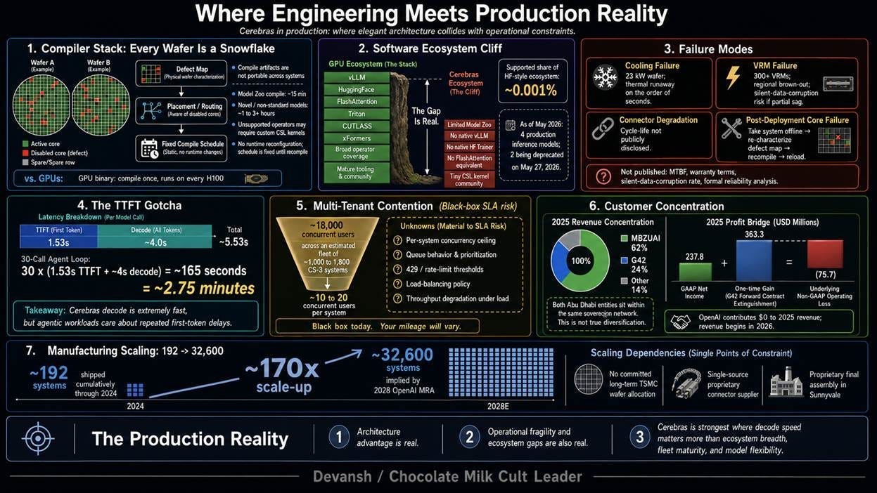
Because Cerebras relies on independent core redundancy to achieve viable manufacturing yields, every wafer possesses a completely unique pattern of roughly 70,000 disabled cores. This makes each chip a physical snowflake, meaning compile binaries are non-portable across a fleet. A binary compiled for one unit cannot run on another because their functional core maps do not line up. If a unit fails, the entire model must be recompiled against the specific defect map of the replacement silicon.
This layout forces the Graph Compiler to calculate all core placement and message routing at compile time. For pre-optimized architectures in Cerebras’s Model Zoo, compilation takes 15 minutes, but custom operators stretch this loop to over 3 hours — and novel architectures frequently fail to compile entirely. When automated compilation fails, engineers must write custom kernels in Cerebras Software Language (CSL), a proprietary model requiring manual coordination of data placement across a physically unique 2D grid. Unlike the GPU ecosystem, which features thousands of CUDA developers contributing optimized open-source kernels, the pool of CSL experts is virtually non-existent.
The Software Ecosystem Cliff
The software isolation of a proprietary platform creates an immediate barrier to standard deployment frameworks. Dominant open-source inference serving frameworks like vLLM do not run on Cerebras hardware. There are no native HuggingFace Trainer integrations, and load-bearing optimization libraries like FlashAttention, Triton, CUTLASS, or xformers do not exist for the platform. As of May 2026, Cerebras supports exactly four models, and two of them — Llama-3.1 8B and Llama-3.3 70B — are scheduled for deprecation on May 27, 2026. While the HuggingFace repository hosts hundreds of thousands of model variants that deploy instantly on NVIDIA hardware, Cerebras supports roughly 0.001 percent of that ecosystem.
Furthermore, proprietary closed-source frontier models are structurally inaccessible to Cerebras, as they remain locked behind their providers’ cloud APIs.
(We are also hit with the inaccessibility of their system to big open weight models as detailed earlier)
What Are the Operational Moats and Trade-offs?
Evaluating the operational model requires balancing where the architecture simplifies infrastructure against where it complicates development. For models smaller than 44 gigabytes, a model fits entirely on a single wafer. This eliminates the distributed-systems complexity of multi-GPU setups, bypassing NVLink topology tuning and NCCL communication failures entirely. Execution is strictly deterministic because the compile schedule is fixed, preventing the non-deterministic numeric drift common in multi-GPU debug loops. Out-of-memory errors are safely trapped at compile time rather than triggering an unpredictable crash 17 hours into a run.
Conversely, the absence of a community kernel ecosystem means developers must independently build unsupported operators from scratch. Tooling is dangerously thin, lacking any granular equivalent to NVIDIA’s Nsight Compute for per-core performance profiling. The long compile loops fundamentally degrade development velocity compared to GPU workflows.
What Are the Physical Failure Modes of Wafer-Scale Systems?
The extreme power and thermal densities of a wafer-scale chip introduce unprecedented operational risks, yet public documentation regarding its reliability metrics remains entirely empty. If the liquid cold plate experiences a localized drop in flow or a loss of surface contact, the WSE-3’s 23-kilowatt power draw allows sub-second time-to-overtemperature limits. The wafer can hit catastrophic thermal damage within seconds before standard datacenter monitoring systems can generate an alert. GPU servers, by contrast, feature long thermal runway and firmware-level automated throttling.
Electrical failures compound this risk. If one of the 300+ voltage regulator modules on the backing board experiences a partial failure, the corresponding reticle zone suffers a local voltage sag. The system cannot dynamically recompile around a localized power brown-out during operation. Instead, this creates a severe silent-data-corruption risk, where local cores generate mathematically incorrect outputs without throwing an explicit hardware error flag. If a core fails permanently post-deployment, the entire machine must be pulled offline to manually re-map the defect layout and run a fresh multi-hour compilation. There is also no public data on how long the proprietary, compliant connector survives the physical shearing forces of 150-to-190-micron thermal expansion cycles.
The Latency Gotchas: Prefill and Multi-Tenant Constraints
Cerebras’s heavy marketing of its 2,100+ tokens-per-second decode speed masks a critical latency flaw: time to first token (TTFT). TTFT requires running a prompt prefill phase, which is not comparably advantaged by the architecture’s sequential design. For a high-reasoning model like gpt-oss-120B, the published TTFT sits at 1.53 seconds.
While an individual user completing a single-turn prompt will not mind a 1.53-second initialization lag, this delay is devastating for agentic workloads. If an autonomous AI agent must chain together 30 sequential LLM calls to complete a multi-step task, the fixed prefill cost multiplies across every iteration, dragging the total loop time to nearly three minutes. In these multi-turn loops, a standard GPU cluster with faster prefill units can deliver comparable total execution times despite generating tokens slower on a per-step basis.
Concurrently, multi-tenant serving introduces strict scaling walls. Cerebras’s pipeline-interleaving mechanism relies on tiny concurrency batch sizes, typically capping a single machine at 10 to 20 concurrent users to avoid bubble latency. At a fleet level, Cerebras’s public API supports roughly 18,000 concurrent users across an estimated deployment of 1,000 to 1,800 active CS-3 machines. Cerebras operates this multi-tenant concurrency model as a complete black box, hiding exact capacity limits, queue behaviors, and rate-limiting thresholds from enterprise buyers.
Sovereign Concentration and Financial Reality
Cerebras’s corporate financial statements reveal extreme customer concentration beneath the high-level metrics. In 2025, a staggering 86 percent of all recognized revenue originated from just two Abu Dhabi entities: the Mohamed bin Zayed University of Artificial Intelligence at 62 percent and G42 at 24 percent. Both operate within the same ultimate state apparatus, meaning this contract value represents an accounting shift rather than genuine market diversification.
Furthermore, the headline 2025 GAAP net income of 237.8 million dollars is entirely driven by a single, non-recurring 363.3-million-dollar accounting gain from the extinguishment of a historical G42 forward contract. Strip this one-time contract adjustment from the books, and the underlying core commercial business operated at a non-GAAP operating loss of 75.7 million dollars. Because the landmark OpenAI agreement contributed zero dollars to recognized 2025 revenue, Cerebras is heading toward its IPO backed by a single sovereign network and a profitability narrative constructed from a one-time book event.
The Manufacturing Scale-Up Risk
Fulfilling the forward order book requires an unprecedented industrial transformation. Cumulatively through the end of 2024, Cerebras has manufactured and shipped approximately 192 total systems. The forward OpenAI infrastructure agreement requires delivering roughly 32,600 systems by 2028 — demanding a 170-fold increase from cumulative lifetime production to an annualized delivery cadence in less than four years.
Every single CS-3 machine requires a full, un-diced 12-inch wafer, yet Cerebras’s public SEC disclosures explicitly state that the company possesses no committed long-term wafer allocation from TSMC. They must compete for limited cleanroom allocations against massive chip buyers like Apple, AMD, Qualcomm, and NVIDIA at TSMC’s most advanced nodes. At the packaging layer, the critical thermal-expansion connector is manufactured under an exclusive, single-source agreement, leaving the entire multi-billion-dollar scale-up exposed to severe supply chain dependencies without the globally distributed networks of its competitors.

Conclusion: Why Did Cerebras Raise at 56 Billion Dollars
Cerebras is wagering on a specific physical reality: that memory bandwidth will dictate the future of inference, and standard GPU packaging cannot scale fast enough to solve it.
If standard High Bandwidth Memory (HBM) improves enough over the next three years to eliminate the decode bottleneck, Cerebras becomes a brilliant but transitional technology.
If it doesn’t — and if single-stream latency becomes the absolute speed limit for agentic AI — Cerebras is positioned exactly where standard architecture physically breaks.
The interesting thing is that Cerebras doesn’t actually need to win the market for their underlying thesis to be right. The industry has already conceded the point. NVIDIA spending 20 billion dollars on Groq, and Google splitting its TPU line into separate training and inference chips, proves that the incumbents know the current hardware is wrong for the job. Starving compute units during decode is a waste. Someone will capture the value of fixing this.
The engineering is real. The physics advantage is quantifiable. The question has never been whether Cerebras built something that works. They did.
The question is whether the market window stays open long enough, and the software ecosystem grows deep enough, for wafer-scale silicon to survive the incumbents it forced into action. And most importantly, how much risk you’re willing to stomach on potentially paradigm-altering bets. Your answer to that determines how much attention you gove this architecture.
Personally, I appreciate that we have a bunch of smart people building difficult things, as opposed to dedicating their lives to Slack Automation, gambling apps, and Ad-tech. That has to stand for something.
Thank you for being here, and I hope you have a wonderful day,
Dev <3
If you liked this article and wish to share it, please refer to the following guidelines.
That is it for this piece. I appreciate your time. As always, if you’re interested in working with me or checking out my other work, my links will be at the end of this email/post. And if you found value in this write-up, I would appreciate you sharing it with more people. It is word-of-mouth referrals like yours that help me grow. The best way to share testimonials is to share articles and tag me in your post so I can see/share it.

Reach out to me
Use the links below to check out my other content, learn more about tutoring, reach out to me about projects, or just to say hi.
Small Snippets about Tech, AI and Machine Learning over here
AI Newsletter- https://artificialintelligencemadesimple.substack.com/
My grandma’s favorite Tech Newsletter- https://codinginterviewsmadesimple.substack.com/
My (imaginary) sister’s favorite MLOps Podcast-
Check out my other articles on Medium. :
https://machine-learning-made-simple.medium.com/
My YouTube: https://www.youtube.com/@ChocolateMilkCultLeader/
Reach out to me on LinkedIn. Let’s connect: https://www.linkedin.com/in/devansh-devansh-516004168/
My Instagram: https://www.instagram.com/iseethings404/
My Twitter: https://twitter.com/Machine01776819
The next global power battle won’t be on land.
It’ll be in space and in the airwaves.
The race is already on:
Satellite networks
Space defense systems
Quantum communications
6G infrastructure
AI-controlled telecom
This isn’t science fiction.
It’s the next layer of global control.
Because in the future:
Who controls space → controls data
Who controls data → controls economies
And 6G?
It won’t just connect phones
It will connect:
Cities
Factories
Military systems
AI networks in real time
The uncomfortable truth:
The next superpowers won’t just dominate on Earth.
They’ll dominate above it.
And most people won’t even realize the shift
Because it’s happening silently, in orbit.
Devansh, this is an absolute masterclass in separating deep-tech physics from venture-backed marketing. Your breakdown of the memory bandwidth wall versus the sheer mechanical brutality of wafer-scale integration is the most lucid analysis of Cerebras on the internet right now.
However, your analysis exposes a terrifying structural vulnerability in these next-generation inference machines—a vulnerability that the industry is entirely ignoring. By focusing purely on throughput and latency, we are building planetary-scale intelligence infrastructure with absolutely zero physical governance.
This is exactly why the Veritas Core Global Truth Substrate is the mandatory next layer for this hardware. If we are moving LLM execution to massive, specialized silicon like the WSE-3, we cannot rely on flimsy software APIs to govern them. Here is how Veritas Core directly solves the catastrophic failure modes you highlighted:
1. Eradicating "Silent Data Corruption"
You correctly pointed out that localized voltage sags on a 23kW wafer can cause cores to generate mathematically incorrect outputs without throwing explicit hardware errors. In high-stakes environments (finance, defense, healthcare), this silent corruption is fatal.
The Veritas Solution: Veritas operates via Runtime-Enforced Verifiable Receipts. Every output generated by the compute layer must be cryptographically hashed and bound to multi-constellation GNSS and Starlink atomic timing before it can leave the node. If a local core suffers a voltage anomaly or data corruption, the cryptographic attestation fails. Our ΣE ontological boundaries physically intercept and drop the corrupted data at the hardware level before it can trigger a real-world consequence.
2. Securing Agentic AI at the Hardware Level
You noted that Cerebras’s time-to-first-token (TTFT) prefill lag is devastating for agentic AI that relies on rapid, multi-turn sequential calls. But as the industry races to optimize hardware for these autonomous agents, we are hurtling toward a cliff: handing unverified software agents the keys to digital and physical infrastructure.
The Veritas Solution: You cannot govern autonomous agents with software classifiers. Veritas implements ABT v1.0 Circuit Breakers directly at the PCIe/hardware boundary. Even if a highly capable agent is running at 2,100 tokens-per-second, it cannot bind a physical or digital action without producing a hardware-attested receipt proving explicit human authorization. We don't slow down the math; we mathematically gate the execution.
3. Shattering the "Black Box" of Multi-Tenant Capacity
Your financial teardown is sobering. Cerebras is heavily reliant on sovereign entities (86% Abu Dhabi concentration) and must dynamically resell idle OpenAI capacity via a "black box" multi-tenant concurrency model to survive negative gross margins.
The Veritas Solution: Compute allocation cannot be a black box managed by a single corporate API, especially when global sovereign interests are involved. Veritas Core utilizes a Maximin Equity Allocation Engine. This Rawlsian optimization matrix enforces equitable, transparent, and mathematically verifiable routing of computing resources. It guarantees that multi-tenant capacity is distributed fairly and transparently, stripping away the ability of monopolies or sovereign states to covertly hoard pipeline resources.
You nailed the premise: hardware problems require hardware solutions. But as we rewrite the physical boundaries of semiconductor memory, we must simultaneously rewrite the physical boundaries of AI custody. Predictive safety and software wrappers are dead. The future of inference must be hardware-anchored truth.