

It takes time to create work that’s clear, independent, and genuinely useful. If you’ve found value in this newsletter, consider becoming a paid subscriber. It helps me dive deeper into research, reach more people, stay free from ads/hidden agendas, and supports my crippling chocolate milk addiction. We run on a “pay what you can” model—so if you believe in the mission, there’s likely a plan that fits (over here).
Every subscription helps me stay independent, avoid clickbait, and focus on depth over noise, and I deeply appreciate everyone who chooses to support our cult.
PS – Supporting this work doesn’t have to come out of your pocket. If you read this as part of your professional development, you can use this email template to request reimbursement for your subscription.
Every month, the Chocolate Milk Cult reaches over a million Builders, Investors, Policy Makers, Leaders, and more. If you’d like to meet other members of our community, please fill out this contact form here (I will never sell your data nor will I make intros w/o your explicit permission)- https://forms.gle/Pi1pGLuS1FmzXoLr6
I recently came across this research on OpenAI’s new Jalapeno chip by Advanced Notes. I appreciated the way it went beyond the (which are very good, as you will see in the table below), to instead provide a complete story on how AI may now be compressing the hardware-design cycle itself. Reading this article felt like a crash course in some of the important things to look out for when it comes to AI for chips.
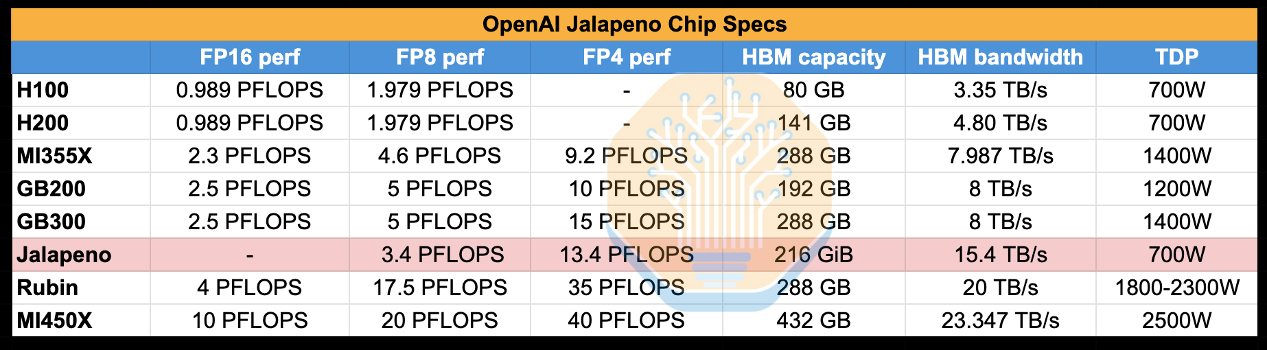
I’ve been thinking about how faster chip design may reduce the cost of being wrong about where AI is going. General-purpose GPUs dominate partly because nobody wants to lock a three-year silicon bet around a workload that may change in six months. If you can bring that cost down enough, we might see a world where GPUs discover the next important workload, after which you might design custom chips to solve that problem more efficiently (assuming it’s important enough). This would likely have some major implications for the market dynamics, software (I anticipate a rise in heterogenous computing), and even in AI/software capabilities(by enabling people to explore new kinds of computational workloads/paradigms that are a bit more awkward on current systems).For eg. take the “An optical neural chip for implementing complex-valued neural network” which drops some serious heat in enabling a more bottom-up development of CVNNs. The authors “highlight an optical neural chip (ONC) that implements truly complex-valued neural networks” w/ superior learning and efficiency.

(Read a lot more about this topic here).
I could see this process enabling more complex valued chips, which can help us explore so many new directions that aren’t feasible today. As someone obsessed w/ researching the structure of intelligence and computation, this implication causes my Hisoka to rise; hence this guest post. As you read it, here are some questions that might be worth playing with:
Is nine months an outlier, or the beginning of a real compression in chip-development timelines?
If custom silicon gets much faster to build, how specialized do chips become?
Who captures the value: hyperscalers, EDA incumbents, startups, or open source?
How powerful does the AI → better hardware → better AI feedback loop become?
I don’t think we know yet. But this piece made me take those questions much more seriously. Hope you’ll enjoy it as much as I did.
1. A Very Hot Jalapeño
Jalapeño, OpenAI’s first custom silicon, was one of the highlights of this week’s Hot Chips conference at Stanford. Richard Ho, OpenAI’s head of hardware, walked the room through benchmark numbers that beat Nvidia’s Blackwell systems on throughput per watt and on latency, and most of the coverage since has understandably focused on that comparison. But what drew my attention was the project timeline: nine months from initial RTL to tapeout.
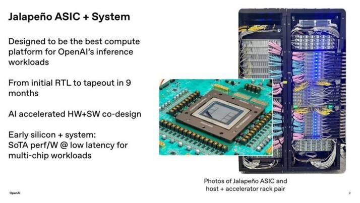
The Jalapeño ASIC and the host-plus-accelerator rack pairing, as shown at Hot Chips 2026. Source: OpenAI.
Nine months is a very aggressive schedule: Jalapeño is built on TSMC’s N3 node, about as leading edge as it gets, and a typical project would take at least 24 months, if not more. That means, the OpenAI team cut the design cycle by somewhere between half and two-thirds.
2. Ho-Ho-Ho...
If you’ve been following Richard Ho for a while, this result shouldn’t feel like it came out of thin air. I first came across his name in 2018, when he co-presented a paper on open source RISC-V verification infrastructure at that year’s RISC-V Summit, and reached out to him afterward to ask more details. There was nothing about AI-accelerated design in that talk, it was standard verification tooling work. But two things about it turned out to matter later: it was open source, and it was about building shared infrastructure rather than a proprietary point solution. Both these habits will resurface later in this story. Looking back at his career since 2018, Google’s TPU program, the Argos video transcoding chip, a short stop at the photonics company Lightmatter, and now OpenAI, there is a fairly consistent thread running through it: someone who has spent close to a decade trying to make chip design move at something closer to software speed. (Coincidentally, my keynote at DVCon Europe back in 2020 was on “What can verification learn from the software world?”)
3. The Prequel: Argos and the First Speed-Up
The first public marker of that thread that I can point to with a paper attached is Argos, a custom video transcoding chip Google built for YouTube. Ho was one of fifty-two co-authors (!) on the 2021 paper describing it, and its most useful section for our purposes is 3.4, on the use of high-level synthesis. Instead of writing RTL by hand, Google’s team described the design in C++ using a commercial HLS tool, Mentor Graphics’ Catapult, paired with an in-house integration layer called Taffel, and reported results that read almost like a pitch for the whole approach: five to ten times less code to write and review, testing throughput multiplied by seven to eight orders of magnitude over conventional RTL simulation, and bugs that used to take weeks to isolate fixed and verified in under a day. Google gave a deeper look at the same project later that year at Hot Chips 33.
Although this was still not leveraging AI in the way we use today, that design flow applied software engineering discipline applied to hardware design. But it is the same underlying bet Ho would keep making for the next five years: that the bottleneck in chip design is process, not physics, and process can be improved and streamlined.
4. I Have a Dream!
The next marker I’d point to is a keynote Ho gave at Synopsys’s SNUG conference in March 2025, titled “Scaling Compute for the Age of Intelligence.” He opened, fittingly, with a bit of personal history: when he first arrived in the Bay Area, his plan was to study AI at Stanford, under Prof. Ed Feigenbaum, one of the founders of the expert-systems field.
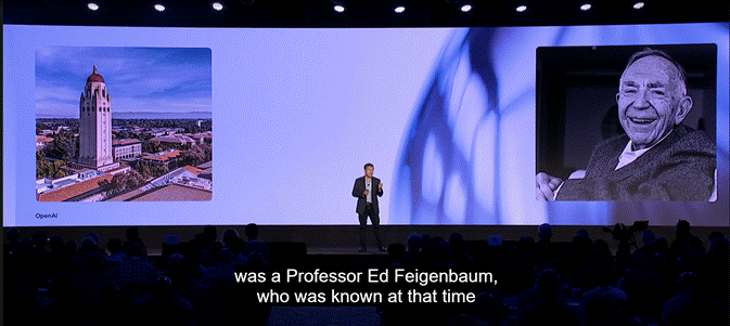
Richard Ho at SNUG 2025, recalling his start at Stanford under Prof. Ed Feigenbaum.
Source: OpenAI/Synopsys.
The keynote spent most of its time on reasoning models and scaling laws before turning, late, to chip design specifically. Ho put up a diagram of the existing flow, architecture, RTL design, logic synthesis, physical design, verification, manufacturing, laid against a hardware development timeline that, by his own account, runs twelve to twenty-four months.
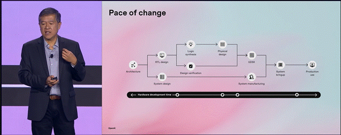
The existing flow, as Ho presented it at SNUG 2025. Source: Synopsys / OpenAI.
Then he put up a second, much simpler diagram and called it his dream: an AI and a human designer in a loop of propose, measure, and optimize, running straight through to production.
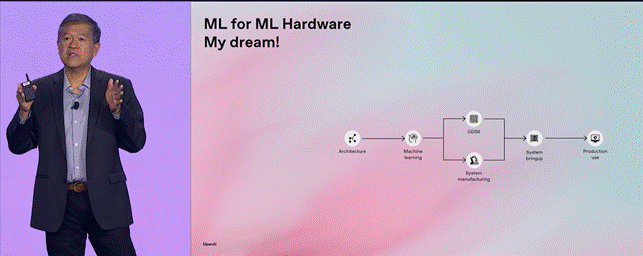
“ML for ML Hardware. My dream!” Source: Synopsys / OpenAI.
Ho was explicit that hardware multi-year timelines sit awkwardly against an ML research cycle that can shift in weeks, a gap borne out by one industry tracker’s release-cadence data, which puts major frontier model releases at roughly four weeks apart by early 2026, down from about six months two years earlier. If model development moves in weeks and chip development moves in years, the chip becomes the constraint on how fast AI itself can improve.
5. Solving Design Bottlenecks
When describing the current flow, Ho said that Verification and Physical Design (two parallel branches in his diagram) are always racing each other, and whichever one takes longer ends up setting the pace for the whole project. So he backed up his proposal for a dream flow with two examples that were already real back then, at least internally at Google. The first was placement, the step where a chip’s largest physical blocks get positioned on the die, using the reinforcement-learning approach published in Nature in 2021 and later commercialized under the name AlphaChip.
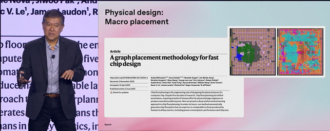
Ho’s placement example: the 2021 Nature paper behind AlphaChip. Source: Synopsys / OpenAI.
The second example was fittingly around verification: Design2Vec, a Google Research verification tool that learns a representation of a chip’s RTL well enough to predict test coverage in seconds instead of running an overnight simulation.
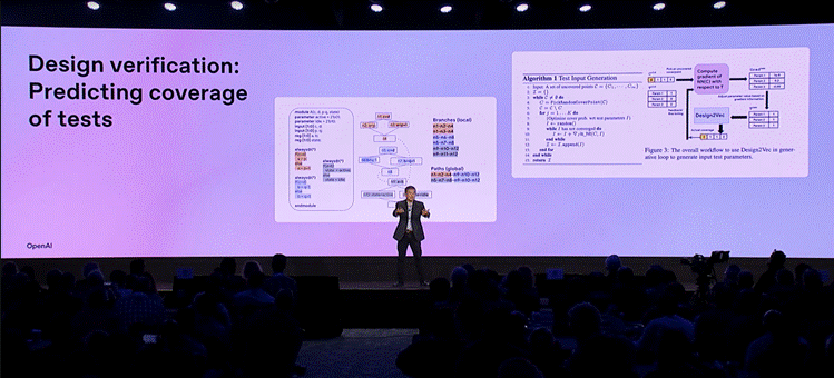
Ho’s verification example: coverage prediction with Design2Vec. Source: Synopsys / OpenAI.
He also mentioned, almost in passing, an experiment closer to home: asking ChatGPT to design a small asynchronous FIFO for clock-domain crossings, a classic interview question from his own early career, and getting back working SystemVerilog along with a UVM testbench and documentation. Not full-chip design, he was careful to say, but a meaningful step.
Two established techniques, plus a glimpse of a third still in its infancy, all resting on the same idea: let a model absorb enough about the design to shortcut a long design cycle.
6. Living the Dream...
Fast forward to August 2026, three OpenAI senior engineers - Richard Ho, Ravi Narayanaswami, and Chris Leary - stand on stage and introduce Jalapeño, a chip that, among its other attributes, was designed in nine months.
Here is the timeline slide they shared in their presentation:
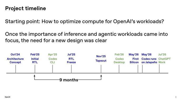
OpenAI’s own project timeline for Jalapeño, presented at Hot Chips 2026. Source: OpenAI.
How did the team achieve this breakthrough design cycle?
Probably Ho’s “dream flow” presented at SNUG was not a distant dream.
Firstly, note the nine months from Initial RTL to Tapeout and the other silicon milestones in blue. Then note the green milestones of OpenAI Codex enabling the faster chip design work. So using Codex to speedup design & verification is a given, probably much beyond the small FIFO use case Ho shared at SNUG.
The second “trick” that Ho showed at SNUG was the AlphaChip placement Reinforcement Learning tool developed at Google.
Now, even if Ho mentioned this AlphaChip work at SNUG while already at OpenAI, I don’t have confirmation that this tool was used in the Jalapeño project.
What I can say: Anna Goldie and Azalia Mirhoseini, the two researchers who built the original AlphaChip placement work at Google, left in 2025 to found Ricursive Intelligence, and are explicitly building a more ambitious, sellable version of that tool for chipmakers and hyperscalers generally, not just Google. Coincidentally, in a TIME100 AI profile published just this week, Anna put the company’s ambition plainly, wanting to take chip design from years down to “months, weeks, maybe even days eventually.” (BTW, we hosted Anna to speak at one of our sessions at the recent DAC)
Separately, and just as speculatively: It just happens that Broadcom, OpenAI’s silicon implementation partner on Jalapeño, is also Google’s TPU partner, a relationship that goes back to 2016 and is now in its seventh generation. MediaTek, which just joined this year as a design partner on Google’s TPU v8 program, has separately built its own version of the AlphaChip placement approach into its most advanced chips, extending the open-sourced technique rather than licensing it commercially. None of that proves anything about Jalapeño specifically, though it does mean the channels through which this kind of technique could move between companies clearly exist, whether or not they were used here.
7. Accelerated HW Synthesis
The one piece of the Jalapeño flow OpenAI did put a name to is XLS (that stands for “Accelerated HW Synthesis”) - a hardware description language that let OpenAI’s own internal models search implementations against measured power, performance, and area, and iterate against a human-optimized baseline. OpenAI’s own slide claims a fifty-six percent improvement on a BF16 multiplier, smaller but still real gains on a couple of other blocks, and major changes landing right up until the day of RTL freeze, the kind of late-stage flexibility that a traditional flow, where physical layout gets locked in early, generally doesn’t allow.
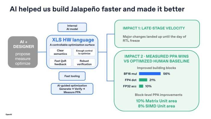
“AI helped us build Jalapeño faster and made it better.” Source: OpenAI, Hot Chips 2026.
Under the hood, XLS is Google’s own open source hardware synthesis toolchain, published on GitHub under an Apache license, and it is in a real sense Argos’s successor: Where Argos’s team wrote in C++ against Catapult, XLS designs are written in a language called DSLX and compiled down, through the toolchain’s own intermediate representation, to Verilog, with an LLVM-based just-in-time compiler standing in for the software-speed simulation that C++ and Catapult provided at Argos. One detail I find genuinely notable: Chris Leary, a listed contributor to the XLS project on GitHub, was one of three presenters, alongside Ho, at Jalapeño’s Hot Chips talk this week, a direct line from Google’s open source tooling into a leading-edge OpenAI and Broadcom tapeout.
It’s also, IMHO, a rather unique choice: Top-tier commercial chip design almost never runs on open source infrastructure, the industry defaults, nearly without exception, to Synopsys, Cadence and Siemens. XLS’s own GitHub page is candid that it remains experimental and is “not an officially supported Google product.” Whatever ran downstream of it for the actual physical implementation on TSMC’s N3 process was almost certainly commercial EDA, since XLS’s own open source path (Yosys and OpenROAD) targets open process kits like SKY130, not leading-edge commercial nodes. But the front end, the layer where OpenAI says its own models did the searching and optimizing, ran through code anyone can read on GitHub today.
The underlying message is that the key chip designers are telling the EDA industry, if you don’t move faster, we’ll find other solutions.
8. Closing the Loop
But beyond the novelty of such an accelerated design cycle, the main insight that is worth sitting with is what it enables.
In the “Project timeline” slide OpenAI showed (see above), they added:
How to optimize compute for OpenAI’s workloads?
Once the importance of inference and agentic workloads came into focus, the need for a new design was clear.
As we already mentioned, Ho said the slow pace of designing chips compared to the fast update of models is a handicap on the silicon side.
OpenAI’s first reasoning model, o1, shipped in September 2024, which is IMHO a plausible trigger for that realization. Reasoning models already require a slightly different type of hardware than “pure” inference, and agentic AI requires further optimization still. OpenAI’s own timeline states that the architecture concept was done in October 2024. By the time of that SNUG keynote, in March 2025, OpenAI was already six weeks into initial RTL work on Jalapeño. Ho, without ever saying so on stage, was already living out the dream flow he had just described to the room.
To fully close the loop, note the May’26 milestone says “Codex runs on Jalapeño.” OpenAI designed silicon that can run ChatGPT optimally, and Codex now runs optimally on this silicon.
Also note that this just in the same month of silicon back – a 1st silicon success!
9. Is This the New Standard Pace?
None of this makes Jalapeño’s nine months a magic trick. It looks more like the payoff of a specific, decade-long institutional habit that moved from Google’s chip teams to OpenAI’s.
I keep asking people, in different occasions, some version of the same question: how much will AI actually compress the chip design cycle – 10%? 50%? 90%?
At the GSA European Executive Forum earlier this summer in Munich, I polled the wide audience, and you can see their opinions in the slide below. Is 50% the new normal or is it just the beginning?
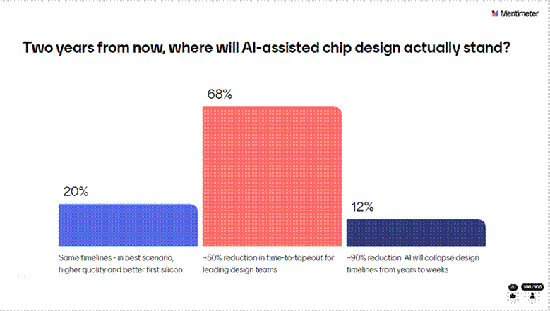
Live poll results from my session at the GSA European Executive Forum, Munich, 2026.
Source: Author’s own poll, Mentimeter.
I also asked four VCs on my DAC panel (including one that invested in Ricursive), and you can read their answers here.
Jalapeño’s timeline slide is, as far as I’ve seen, the first public answer that comes with a number large enough to take seriously.
It also leaves a question I didn’t set out to answer here: who actually owns this new layer of tooling (EDA? Startups? Open-source?), and what happens to the rest of the EDA industry if AI-driven design flows become standard practice rather than a Hot Chips keynote slide.
Thank you for being here, and I hope you have a wonderful day.
Dev <3
I provide various consulting and advisory services. If you‘d like to explore how we can work together, reach out to me through any of my socials over here or reply to this email.
I put a lot of work into writing this newsletter. To do so, I rely on you for support. If a few more people choose to become paid subscribers, the Chocolate Milk Cult can continue to provide high-quality and accessible education and opportunities to anyone who needs it. If you think this mission is worth contributing to, please consider a premium subscription. You can do so for less than the cost of a Netflix Subscription (pay what you want here).

If you liked this article and wish to share it, please refer to the following guidelines.
That is it for this piece. I appreciate your time. As always, if you’re interested in working with me or checking out my other work, my links will be at the end of this email/post. And if you found value in this write-up, I would appreciate you sharing it with more people. It is word-of-mouth referrals like yours that help me grow. The best way to share testimonials is to share articles and tag me in your post so I can see/share it.
Reach out to me
Use the links below to check out my other content, learn more about tutoring, reach out to me about projects, or just to say hi.
Small Snippets about Tech, AI and Machine Learning over here
AI Newsletter- https://artificialintelligencemadesimple.substack.com/
My grandma’s favorite Tech Newsletter- https://codinginterviewsmadesimple.substack.com/
My (imaginary) sister’s favorite MLOps Podcast-
https://machine-learning-made-simple.medium.com/
My YouTube: https://www.youtube.com/@ChocolateMilkCultLeader/
Reach out to me on LinkedIn. Let’s connect: https://www.linkedin.com/in/devansh-devansh-516004168/
My Instagram: https://www.instagram.com/iseethings404/
My Twitter: https://twitter.com/Machine01776819
Hi Everyone!
I’ve recently started a new Substack called “Learn Daily,” where I’ll be sharing something new every day on topics like finance, business, books, habits, health, and more.
I’d love for you to check it out and share your feedback. And if you find the content interesting or useful, please consider subscribing!
Looking forward to learning and growing together.
https://learndailyy.substack.com/p/the-mechanics-of-real-rest?r=rtelv&utm_campaign=post&utm_medium=web&showWelcomeOnShare=true