
Inside the AI Hardware Race [Guest]
Everything you need to know about CPU, GPU, TPU, ASICs, APU, NPU and others, unpacking the meaning behind these abbreviations

It takes time to create work that’s clear, independent, and genuinely useful. If you’ve found value in this newsletter, consider becoming a paid subscriber. It helps me dive deeper into research, reach more people, stay free from ads/hidden agendas, and supports my crippling chocolate milk addiction. We run on a “pay what you can” model—so if you believe in the mission, there’s likely a plan that fits (over here).
Every subscription helps me stay independent, avoid clickbait, and focus on depth over noise, and I deeply appreciate everyone who chooses to support our cult.
PS – Supporting this work doesn’t have to come out of your pocket. If you read this as part of your professional development, you can use this email template to request reimbursement for your subscription.
Every month, the Chocolate Milk Cult reaches over a million Builders, Investors, Policy Makers, Leaders, and more. If you’d like to meet other members of our community, please fill out this contact form here (I will never sell your data nor will I make intros w/o your explicit permission)- https://forms.gle/Pi1pGLuS1FmzXoLr6
With all the news about Nvidia hitting 5 trillion USD Market Cap, it’s now a good time to ask a simple question: what makes Nvidia so profitable? The simple answer, their hold on GPUs, raises two more questions: Why are GPUs so good for AI? And will they continue to be dominant, or will other chips rise to take their place?
Written by the Turing Post team (Ksenia Se and Alyona Vert) – today’s guest post will prime you to start your journey into this question. Ksenia is one of AI’s most respected journalists and researchers. If you read me, you know how often I share her thoughtful analysis. She built Turing Post into one of the sharpest publications tracking the global AI ecosystem - read weekly by leaders like me, top execs at NVIDIA, Eric Schmidt, and the Hugging Face founders. Her work has become essential reading for anyone trying to see the shape of AI’s next phase: not only the models, but the machines underneath them.
That’s where this guest post comes in. Together, we map the full terrain of AI hardware—from the classic CPU, GPU, and TPU to the rising architectures shaping what comes after: wafer-scale ASICs like Cerebras, custom hyperscaler chips from AWS, hybrid APUs, edge-focused NPUs, and experimental designs such as RPUs and neuromorphic processors. The goal isn’t to list acronyms—it’s to understand what each design means for the future of intelligence: where computation happens, how power is consumed, and who controls the stack.
By the end, you’ll see how the AI hardware world is fragmenting, where the real breakthroughs might come from, and why the GPU era—while not over—has already started to splinter.
As you read, consider the following:
How does each hardware type redefine the relationship between compute and memory?
What does “AI hardware fragmentation” actually mean for developers, startups and national strategies?
Are we witnessing a diversification of tools, or the beginning of a new monopoly under different physics?
Even a child now knows what a GPU (Graphics Processing Unit) is – thanks to AI and to Nvidia, which keeps pushing its chips relentlessly. Of course, hardware is both the stumbling block and the engine that powers models and runs their tech stack. But why is the conversation so fixated on GPUs alone? Are there other contenders that could shape the future of AI hardware? CPUs and TPUs, sure – but is that all?
Today, let’s break out of the GPU bubble and look beyond the familiar trio of GPUs, CPUs, and TPUs. Developers around the world have been working on alternative designs, each promising new efficiencies and fresh approaches.
We wanted to create a full guide on AI hardware for you, so let’s start with the three main giants and move to something less popular but not less interesting from the inside: custom-built ASICs like Cerebras WSE and AWS hardware; APUs, NPUs, IPUs, RPUs, and FPGAs. We’ll make sense of all of these terms, so you can capture the full picture of AI hardware. It’s going to be a very insightful read!
In today’s episode, we will cover:
CPU, GPU, TPU – three core hardware designs
Central Processing Unit (CPU)
Graphics Processing Unit (GPU)
Tensor Processing Unit (TPU)
Application-Specific Integrated Circuits (ASICs)
Cerebras Wafer-Scale Engine (WSE)
AWS Trainium and AWS Inferentia
Accelerated Processing Unit (APU)
Neural Processing Unit (NPU)
Other promising alternative architectures
Intelligence Processing Unit (IPU)
Resistive Processing Unit (RPU)
Field-Programmable Gate Arrays (FPGAs)
Emerging Architectures
Conclusion
Sources and further reading
CPU, GPU, TPU – three core hardware designs
Before we move to the alternatives lets break down what these notorious CPU, GPU and TPU are.
These three giants are Processing Units (PUs) – specialized electronic circuits that execute instructions from software programs for computation. Many call them the “brain” of a computer system. PUs perform different arithmetic, logic, controlling, and input/output operations to process data, transforming it into useful information.
The main PUs types are optimized for different types of workloads →
Central Processing Unit (CPU)
Central Processing Unit (CPU) is developed for general-purpose computing and sequential task execution.
CPU is simply the oldest. The story of CPU’s predecessor begins in 1945 with ENIAC, Electronic Numerical Integrator and Computer, introduced by John Mauchly and J. Presper Eckert Jr. It was the first ever programmable, electronic, general-purpose digital computer, that could solve a wide range of numerical problems through reprogramming, using 18,000 vacuum tubes.
The same year came John von Neumann’s “First Draft of a Report on the EDVAC”, proposing storing both data and instructions in the same memory. This stored-program model became the template for modern CPUs.
In mid-1950s, vacuum tubes were replaced by transistors. From that moment, processors were built out of many transistor-based components spread across circuit boards, making computers smaller, faster and less power-hungry.
In 1960s integrated circuits (ICs) appeared, packing multiple transistors onto a single silicon chip. And finally, in 1971, Intel released the 4004, the world’s first commercial microprocessor, a 4-bit CPU on a single chip. This was the true birth of the modern CPU.
Intel 8086 is the ancestor of today’s x86 CPUs, and up-to-date solution for modern efficiency is multi-core processors – multiple CPUs on one chip.
So what is inside up-to-date CPUs and how do they work?
At the heart of a CPU is the control unit with complex circuits that control the computer by sending out electrical signals, direct data and instructions to the right places. The arithmetic logic unit (ALU) handles math and logical operations, while registers and cache provide tiny but super-fast storage areas for data the processor needs constantly.
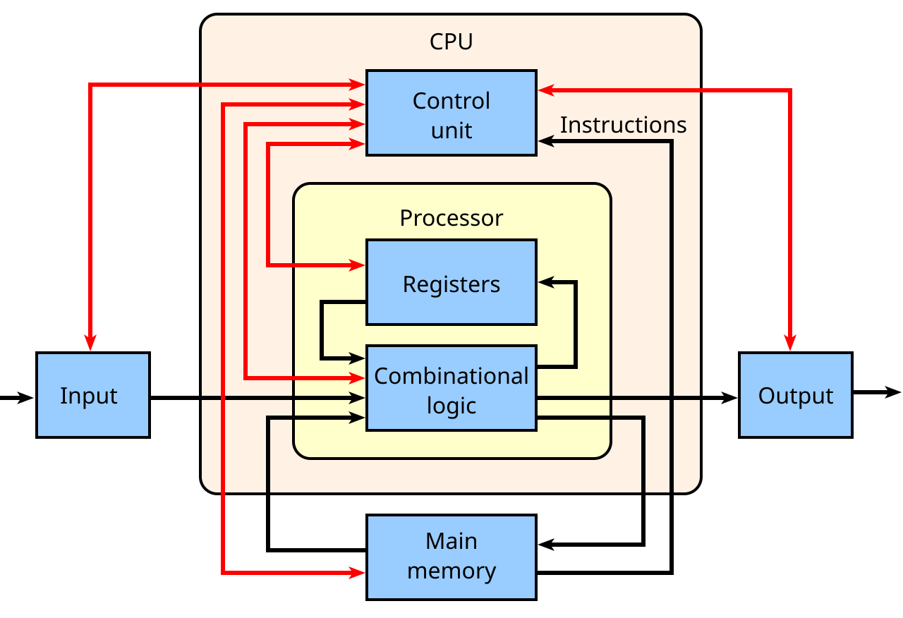
Image Credit: Wikipedia
The CPU also contains cores – processing units in the CPU itself, each of which can independently process instructions, and threads, which allow a core to juggle multiple instruction streams. All of this runs to the beat of the clock, which provides the rhythm that keeps everything in sync. Supporting components like buses (for data transfer) and the instruction register and pointer (to track what’s next) tie the system together so instructions can move smoothly from one step to the next.
The CPU operates on a simple but powerful cycle: fetch → decode → execute.
It fetches data or instructions from memory,
Decodes them into signals the hardware understands,
Executes the required operations (e.g. calculation solving, comparing values, or sending data somewhere else).
This happens billions of times per second in modern processors, with multiple cores and threads working in parallel to boost performance, making CPU like a highly organized team of components. Fewer cores (1-2) in CPU leads to efficiency, while more cores are used to power high-performance tasks.
Today’s CPUs mainly come from:
Intel, which makes Core (consumer), Xeon (server/workstation), Pentium and Celeron (budget) chips;
AMD, that offers Ryzen (consumer/high-performance) and EPYC (server) processors along with APUs (Accelerated Processing Unit) that combine CPU and GPU on one chip (we will look at them later below).
The main problem with CPUs for AI is that they’re optimized for sequential, general-purpose tasks rather than massively parallel matrix operations, making them far slower and less efficient than GPUs or specialized chips.
So let’s move to the second chip on our timeline – the famous GPUs.
Graphics Processing Unit (GPU)
Graphics Processing Unit (GPU) is optimized for massively parallel data processing with high throughput. Originally GPUs were invented to accelerate computer graphics in images and videos, but later they turned out to be useful in non-graphic calculations. Now they are broadly used in parallelizable workloads like handling data-intensive tasks and training of AI models.
Today GPUs are the main driver of AI performance and a key benchmark of computational capacity in AI.
The term Graphics Processing Unit (GPU) was officially introduced by NVIDIA in 1999 with the release of the GeForce 256. NVIDIA called it the world’s first GPU, and the official definition is “a single-chip processor with integrated transform, lighting, triangle setup/clipping, and rendering engines.”
So how does the legendary GPU work? →
Inside a GPU, you’ll find billions of tiny transistors etched onto a silicon chip, arranged into thousands of lightweight processing cores. These cores are connected by intricate wiring and supported by high-bandwidth memory and cache, allowing data to flow rapidly between them. The whole package is sealed with protective materials and cooling systems to keep it stable.
(One of the greatest book to read about the history of chips is “Chip War: The Fight for the World’s Most Critical Technology” by Chris Miller. Highly recommended.)
Unlike a CPU, a GPU is built for parallelism – it splits a big job into thousands of smaller, independent tasks and distributes them across their cores, so they’re all computed simultaneously. That’s why GPUs are perfect for training and running AI models, which involve repetitive matrix and tensor calculations on enormous datasets. Thanks to GPU’s parallel architecture, training can happen in days instead of months, and inference can be fast enough for real-time use in chatbots, for example.
The global leader in GPU production is NVIDIA, which created the entire parallel computing platform, called CUDA (Compute Unified Device Architecture), that unlocks the GPU hardware for general-purpose computing and makes the GPU programming accessible.
The main AI infrastructure and industry GPUs from NVIDIA include:
V100 (Volta) – explicitly designed for deep learning acceleration. It introduced Tensor Cores – specialized hardware units that accelerate matrix operations for AI training.
A100 (Ampere) – has more Tensor Cores, better memory bandwidth, and support for multi-instance GPU (MIG). It allows splitting one physical GPU into several logical GPUs for efficiency.
H100, H200 (Hopper) – industry standard for AI. H series deliver transformer engine support, massive memory bandwidth, and high-level speed for training and inference.

Image Credit: NVIDIA H100 NVL GPU Product Brief
Blackwell (e.g., B200 and GB200 Grace-Blackwell ‘superchip’) is designed for next-gen AI models with tens of trillions of parameters. As the successor to Hopper, it introduces FP4 precision and delivers major inference throughput gains, especially for massive transformer workloads.
As the industry needs more processors specialized for AI, here come the next core type of hardware – TPUs.
Tensor Processing Unit (TPU)
Tensor Processing Unit (TPU) is a custom-built chip, designed by Google specifically for accelerating neural network operations, especially matrix multiplications and machine learning workflows. It was firstly presented at Google I/O 2016 and falls into the category of ASICs – Application-Specific Integrated Circuits (ASICs). TPU has the following basic architecture:
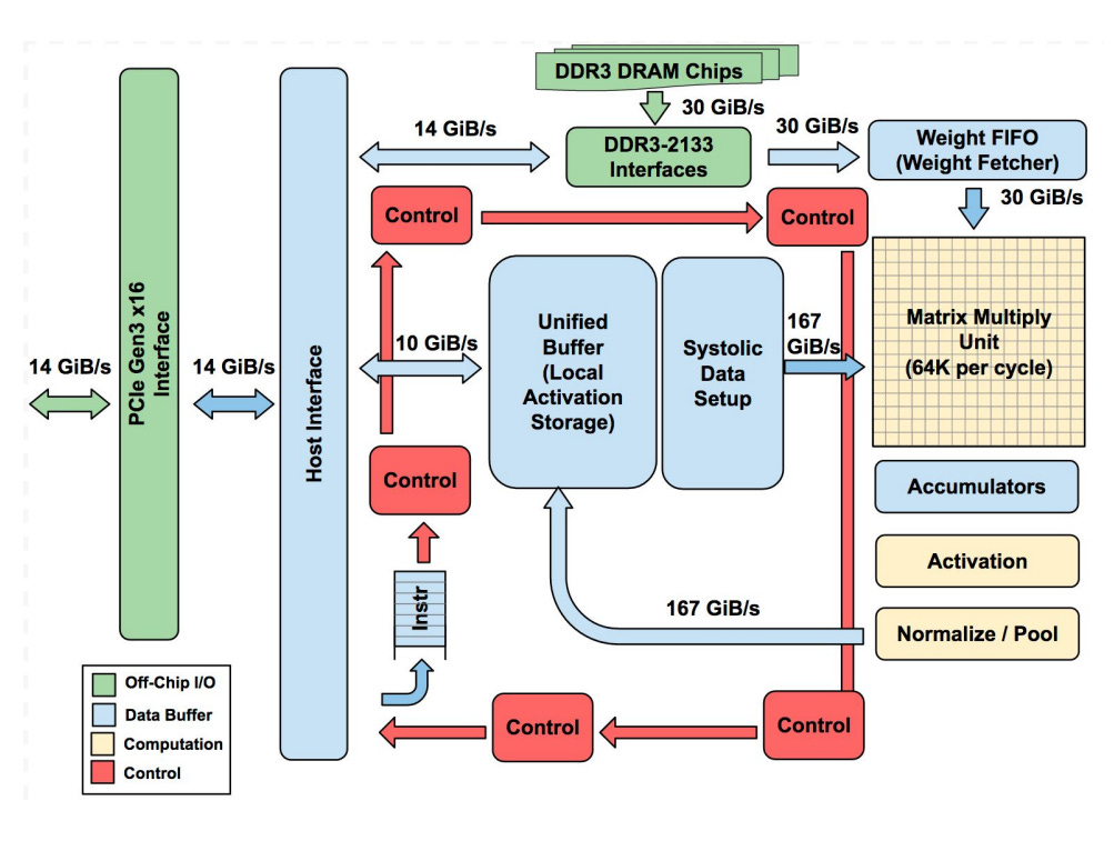
Image Credit: “In-Datacenter Performance Analysis of a Tensor Processing Unit” paper
The star component is the Matrix Multiply Unit – a giant 256×256 array of multiply-accumulate cells (MACs) arranged in a systolic array, where data flows in waves through the grid.
The TPU also has large on-chip memories:
A Unified Buffer (24 MB) to hold intermediate activations;
Weight Memory/FIFOs for neural network weights;
Accumulators (4 MB) to collect sums.
Control logic, PCIe interfaces, and activation units (for functions like ReLU or sigmoid) support the matrix engine, but most of the chip is dedicated to raw compute and fast data movement.
The main feature is that TPU works as a coprocessor:
The host CPU sends it instructions over PCIe, and the TPU executes them directly.
Its instruction set is small (about a dozen commands), and the hardware pipelines everything so the Matrix Unit is always busy. Frameworks like TensorFlow compile models into these low-level instructions.
256 small on-chip memories (distributed accumulator RAMs) collect the partial sums, while the systolic array does multiply-accumulate (MAC) operations. By streaming weights/data into the systolic array and reusing them locally in on-chip buffers, TPUs minimize off-chip memory access. As a result, most of the computation, layer by layer, runs directly on the chip.
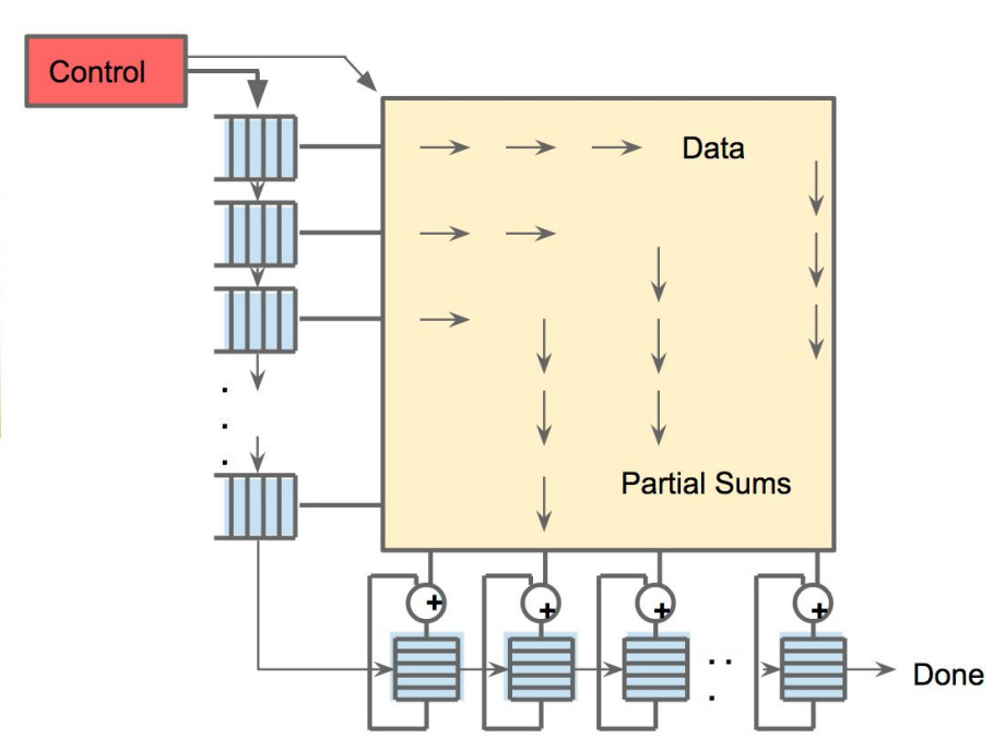
Image Credit: “In-Datacenter Performance Analysis of a Tensor Processing Unit” paper
To sum up, each unit in TPU does small calculations and passes partial results along, saving power and dramatically speeding up the math behind AI models. This is why TPUs achieve high throughput while using much less power than CPUs/GPUs for the same task. According to Google’s 2017 analysis, TPUs achieved ~30–80× better performance per watt compared to contemporary CPUs and GPUs (measured on inference workloads vs K80-class GPUs).
But with only these three types of hardware, we can’t get a complete picture of what powers AI everywhere. So we should also define what the entire field has to offer us. As TPUs are the part of ASIC-based AI chips, we will start our exploration of powerful alternatives with this group. So let’s unpack how they see the future →
Application-Specific Integrated Circuits (ASICs)
ASICs are fully custom-built silicon chips designed for one targeted AI workload. This group includes hyperscaler chips and startups building dedicated AI hardware. In this section, we can’t avoid mentioning…
Cerebras Wafer-Scale Engine (WSE)
Cerebras sees the future in wafer scale. Their latest Cerebras WSE-3 chip is actually one of the largest AI chip ever built – it is 46,255 mm². The key technology is that Cerebras turns a whole silicon wafer into one chip unlike cutting it wafer into hundreds of small processors, as it is done for CPUs or GPUs.
WSE-3 contains 4 trillion transistors, 900,000 AI-optimized cores, and 44 GB of on-chip SRAM memory. Each core has its own local memory, and they are all linked together by an ultra-high bandwidth fabric that spans the wafer, so the compute and memory are brought closer together.

Image Credit: Cerebras Wafer-Scale Engine (WSE) datasheet
Cerebras’ wafer scale idea brings really impressive results:
A single WSE-3 delivers 125 petaFLOPS of AI compute.
As Cerebras claim, combining WSE-3 into a Wafer-Scale Cluster (WSC) with integrated MemoryX (off-chip storage for giant model weights) and SwarmX (for broadcasting weights and aggregating gradients across nodes) lets scale to multi-trillion parameter models with near-linear efficiency, avoiding the complex communication overhead of traditional GPU clusters.
What models now run on Cerebras WSE? Here are two illustrative examples:
Alibaba’s Qwen3 Coder 480B Instruct, reaching 2,000 tokens per second speed.
Mixture-of-Experts (MoE) models: Cerebras makes them much easier and efficient to train at scale. These models can be trained on a single device without model parallelism, which is usually needed when using GPUs. Batch Tiling on Attention (BTA) addresses the compute inefficiency of sparse MoE models, decoupling batch size requirements between attention and expert layers. This way attention runs on smaller tiles to reduce memory pressure, and expert networks see larger effective batches to keep their cores busy.
So this is a powerful technology, and its power is its scale.
AWS Trainium and AWS Inferentia
Amazon also has their alternative to GPU dominance and so their own vision of building effective hardware. Their two in-house chips are designed specifically for AI workloads and are deeply integrated into the AWS ecosystem.
AWS Trainium is created for training models and AWS Inferentia – for inference. Inside, both families use custom NeuronCores, high-bandwidth memory (HBM), and dedicated engines for tensor math, collective communication, and sparsity acceleration.
Trainium 2 UltraServer, featuring 64 Trainium 2 chips, can deliver up to 83.2 petaflops of FP8 compute for sparse models, or about 20.8 petaflops for dense FP8 workloads, compared to NVIDIA H100’s ~4 petaflops of FP8 compute per GPU.
AWS Inferentia 2 allows deployment of LLMs and diffusion models at scale with up to ~50% better performance per watt than comparable EC2/GPU-based instances (e.g., G5).
So AWS hardware provides the solid combination of scale, performance, and cost efficiency for the demands of generative AI.
From the examples of customized efficient ASICs we return to the promising hardware groups with this “..PU” in their names. And here is…
Accelerated Processing Unit (APU)
As we’ve already mentioned, AMD developed a mixed architecture of PU, fusing CPU and GPU capabilities into a single package. This resulted in Accelerated Processing Unit (APU) that removes the bottleneck of shuttling data back and forth between separate processors.
The AMD Instinct MI300A is the biggest example of this idea so far. It packs 24 ‘Zen 4’ CPU cores, 228 GPU compute units, and a huge 128 GB of HBM3 memory.
Under the hood, it’s built using AMD’s chiplet and 3D stacking tech. The MI300A’s memory is coherently shared between CPU and GPU, delivering 5.3 TB/s peak bandwidth. Its multi-chip architecture uses chiplets and die stacking to place CPU and GPU compute units right next to the high-bandwidth memory, with everything tied together by AMD’s Infinity Fabric and Infinity Cache. This chip also supports all the key AI data formats and has hardware support for sparsity.
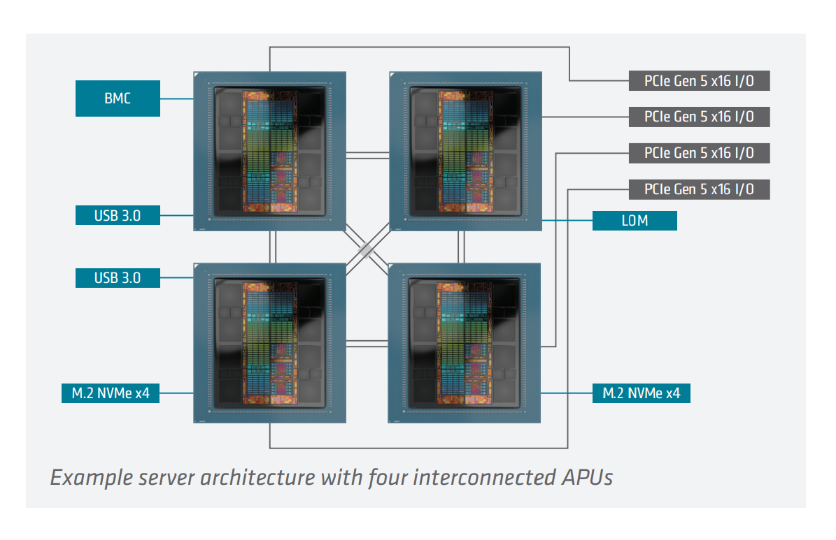
Image Credit: AMD INSTINCT™ MI300A APU Datasheet
So really, why choose between CPU and GPU if you can get “all-in-one engine”?
NVIDIA also supports this concept in its NVIDIA Grace Hopper Superchip – a unified module that pairs an Arm-based Grace CPU with a Hopper GPU, using NVIDIA’s NVLink-C2C chip-to-chip interconnect. The main benefits are the same as for AMD’s MI300A:
CPU and GPU threads can directly access each other’s memory,
they can perform atomic operations, and
manage synchronization more efficiently.
NVIDIA reports Grace Hopper Superchip achieves up to 8× faster training of graph neural networks (GNNs) versus H100 GPUs connected via PCIe, and ~30× faster embedding generation compared to CPU-only baselines.
However, this blending of CPU and GPU comes with higher power draw, less flexibility, and complex manufacturing.
Our next stop is some more tiny hardware stuff.
Neural Processing Unit (NPU)
Imagine the idea that you have an accelerator in an ordinary chip specifically for AI tasks. This is what Neural Processing Units (NPUs) are about. NPUs are basically little engine inside modern chips that are built just for running AI stuff – things like neural networks, image and speech recognition, or even local LLMs. Mimicking the human brain’s neural network architecture, NPUs are tuned specifically for the patterns of AI workloads: lots of matrix multiplications, activations, and data moving around fast with minimal power use.
Here are some examples you can actually find in devices today:
Qualcomm Hexagon NPU inside Snapdragon chips, powering AI features in smartphones, cars, wearable devices, etc.
The Apple Neural Engine that was first introduced in the A11 Bionic chip (2017) and now is embedded in every iPhone, iPad, and Mac with Apple silicon, where it powers FaceID, image processing, and Siri.
Intel’s NPU in their new Core Ultra AI PC processors (Lunar Lake, Arrow Lake). It is made to handle Windows Copilot+ features locally.
AMD’s XDNA / XDNA 2 NPU shows up in Ryzen AI processors for laptops, hitting up to 55 TOPS of AI performance.
NPUs are really great for on-device inference, but they are not powerful enough for training LLMs or running really heavy workloads. They also can’t replace a CPU or GPU for general tasks, and if you run something that isn’t a neural net, NPUs just won’t work properly. This narrow specialization is what makes NPU special among other PUs.
Other promising alternative architectures
Intelligence Processing Unit (IPU)
Graphcore’s IPU is a massively parallel processor with 1,472 independent processor cores running nearly 9,000 parallel threads all closely tied to 900MB of fast In-Processor Memory. This means data can be processed right where it’s stored. IPU is designed specifically for machine learning workloads. With a high degree of fine-grained parallelism and on-chip memory architecture, it excels at graph-based computation and handling irregular and sparse workloads by executing operations across graph nodes in parallel.
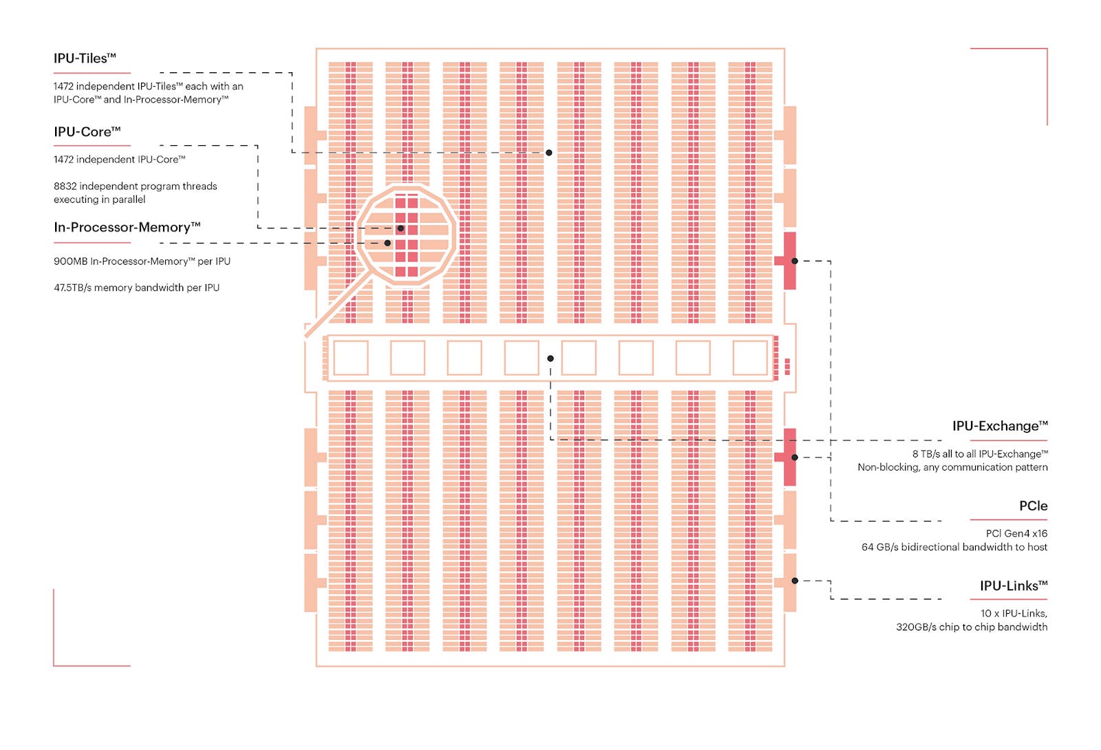
Image Credit: the Colossus™ MK2 GC200 IPU, Graphcore IPU blog
Resistive Processing Unit (RPU)
RPUs are experimental in-memory compute units using resistive memory, like memristors or RRAM, to perform matrix operations directly within memory arrays. This approach minimizes data movement, potentially reducing energy and latency. In 2025, researchers from IBM presented analog in-memory AI accelerators using ReRAM that support on-chip training and inference, with low-voltage switching and multi-bit capacity.
Field-Programmable Gate Arrays (FPGAs)
This hardware is important for reconfigurable AI, especially when you want full control over parallelism, memory, and latency. Unlike GPUs or ASICs, you can tailor an FPGA to your model’s exact needs, and update it later if your architecture changes.
A good example here is AMD Versal™ AI Edge Series Gen 2 that belongs to AMD’s adaptive SoC (System-on-Chip) family. It builds on classic FPGA programmable logic but also integrates Arm CPUs and specialized AI Engines on the same die.
Emerging Architectures
Quantum Processors
Quantum chips use qubits instead of classical bits, exploiting superposition and entanglement. They’re being tested for optimization, search, and simulation tasks – areas where quantum mechanics can offer a theoretical speedup. But qubits remain fragile and noisy, so current quantum machines are limited to toy problems. For now, they’re a long-term moonshot, not a replacement for GPUs or ASICs.
Processing-in-Memory (PIM) & MRAM-based Chips
One of AI’s biggest bottlenecks is moving data between memory and compute. PIM integrates compute directly into memory arrays, cutting this back-and-forth. MRAM (magnetic RAM) is a promising non-volatile memory technology that can support this shift, enabling denser and more energy-efficient accelerators. Companies like Samsung and startups such as Mythic are experimenting with prototypes. PIM isn’t science fiction – it could realistically enter datacenters and edge devices in the next decade.
Neuromorphic Chips
Neuromorphic processors are inspired by the brain’s spiking neurons. Instead of dense, clock-driven matrix multiplications, they rely on sparse, event-driven spikes. Chips like Intel’s Loihi and IBM’s TrueNorth aim to deliver ultra-low-power intelligence, especially for sensors, IoT, and robotics. Their challenge: software and algorithms for spiking neural networks are still immature. Neuromorphic hardware could excel at low-power edge AI, but it remains unclear whether it will scale to workloads like large transformers.
Conclusion
Overall, what do we have for each of the hardware type?
CPU (Central Processing Unit) – general-purpose processor.
GPU (Graphics Processing Unit) – specialized for parallel graphics/math workloads.
TPU (Tensor Processing Unit) – Google’s AI accelerator.
ASICs (Application-Specific Integrated Circuits) – custom-built AI chips for targeted AI workload.
APU (Accelerated Processing Unit) – AMD’s CPU + GPU hybrid.
NPU (Neural Processing Unit) – tiny chips optimized for AI/ML inference on-device.
IPU (Intelligence Processing Unit) – provides high degree of fine-grained parallelism and on-chip memory architecture.
RPU (Resistive Processing Unit) – in-memory compute units using resistive memory.
FPGAs (Field-Programmable Gate Arrays) – for full control over parallelism, memory, and latency.
As you can see, there are many PU options and some alternatives to GPUs that make the hardware landscape diverse and open to future breakthroughs from many sides. Recently, many big companies announced that they are cooking something new: NVIDIA working on Rubin architecture, Meta testing its in-house chips, Alibaba and other Chinese companies developing AI inference chips to build their own hardware ecosystems, etc. And this means more new tech stacks brought to the table.
If we look beyond the GPUs and CPUs we can notice the trend of increasing fragmentation of the AI hardware market, with each player pushing its own ecosystem. For developers and enterprises this is a challenge to navigate compatibility, software support, and cost-efficiency across this expanding hardware landscape.
Sources and further reading
CPUs
What is a central processing unit (CPU)? (IBM blog post)
Types of central processing units (CPUs) (IBM blog post)
GPUs
What is a GPU and its role in AI? (Google Cloud documentation)
Multi-GPU Workflows (NVIDIA guide)
CUDA C++ Programming Guide (NVIDIA guide)
NVIDIA Hopper Architecture In-Depth (NVIDIA blog post)
NVIDIA H100 NVL GPU (Product Brief)
NVIDIA Blackwell Architecture (NVIDIA blog post)
TPUs
In-Datacenter Performance Analysis of a Tensor Processing Unit (Google paper, 2017)
TPU architecture (Google Cloud documentation)
An in-depth look at Google’s first Tensor Processing Unit (TPU)
ASICs
APUs
AMD INSTINCT™ MI300A APU (Datasheet)
NVIDIA GH200 Grace Hopper Superchip (NVIDIA blog post)
NPUs
QUALCOMM HEXAGON NPU: Powering the generative AI revolution (Qualcomm blog post)
Deploying Transformers on the Apple Neural Engine (Apple blog post)
IPUs
INTELLIGENCE PROCESSING UNIT (Graphcore blog)
RPUs
FPGAs
Emerging architectures
Quantum computing and artificial intelligence: status and perspectives
PIM-AI: A Novel Architecture for High-Efficiency LLM Inference
Roadmap to Neuromorphic Computing with Emerging Technologies
Resources from Turing Post
Thank you for being here, and I hope you have a wonderful day.
Dev <3
I provide various consulting and advisory services. If you‘d like to explore how we can work together, reach out to me through any of my socials over here or reply to this email.
I put a lot of work into writing this newsletter. To do so, I rely on you for support. If a few more people choose to become paid subscribers, the Chocolate Milk Cult can continue to provide high-quality and accessible education and opportunities to anyone who needs it. If you think this mission is worth contributing to, please consider a premium subscription. You can do so for less than the cost of a Netflix Subscription (pay what you want here).
If you liked this article and wish to share it, please refer to the following guidelines.
That is it for this piece. I appreciate your time. As always, if you’re interested in working with me or checking out my other work, my links will be at the end of this email/post. And if you found value in this write-up, I would appreciate you sharing it with more people. It is word-of-mouth referrals like yours that help me grow. The best way to share testimonials is to share articles and tag me in your post so I can see/share it.
Reach out to me
Use the links below to check out my other content, learn more about tutoring, reach out to me about projects, or just to say hi.
Small Snippets about Tech, AI and Machine Learning over here
AI Newsletter- https://artificialintelligencemadesimple.substack.com/
My grandma’s favorite Tech Newsletter- https://codinginterviewsmadesimple.substack.com/
My (imaginary) sister’s favorite MLOps Podcast-
https://machine-learning-made-simple.medium.com/
My YouTube: https://www.youtube.com/@ChocolateMilkCultLeader/
Reach out to me on LinkedIn. Let’s connect: https://www.linkedin.com/in/devansh-devansh-516004168/
My Instagram: https://www.instagram.com/iseethings404/
My Twitter: https://twitter.com/Machine01776819
Thank you! The hardware side of things is super interesting. I’m reading “Chip Wars” right now. Learning about the supply chain is fascinating.
the supply chain is at the core of everything